 | –≠–ª–µ–∫—Ç—Ä–æ–Ω–Ω—ã–π –∫–æ–º–ø–æ–Ω–µ–Ω—Ç: 74AC174SJ | –°–∫–∞—á–∞—Ç—å:  PDF PDF  ZIP ZIP |
© 1999 Fairchild Semiconductor Corporation
DS009935
www.fairchildsemi.com
November 1988
Revised November 1999
7
4
AC
1
74 ∑
74ACT174
Hex D-
T
y
pe Fl
ip
-Fl
op wi
th
M
a
ster
Reset
74AC174 ∑ 74ACT174
Hex D-Type Flip-Flop with Master Reset
General Description
The AC/ACT174 is a high-speed hex D-type flip-flop. The
device is used primarily as a 6-bit edge-triggered storage
register. The information on the D inputs is transferred to
storage during the LOW-to-HIGH clock transition. The
device has a Master Reset to simultaneously clear all flip-
flops.
Features
s
I
CC
reduced by 50%
s
Outputs source/sink 24 mA
s
ACT174 has TTL-compatible inputs
Ordering Code:
Device also available in Tape and Reel. Specify by appending suffix letter "X" to the ordering code.
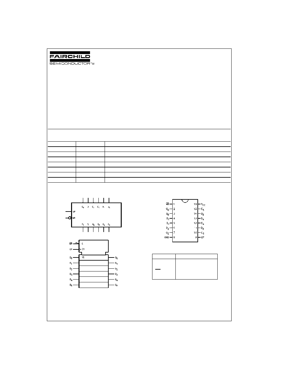
Logic Symbols
IEEE/IEC
Connection Diagram
Pin Descriptions
FACT
is a trademark of Fairchild Semiconductor Corporation.
Order Number
Package Number
Package Description
74AC174SC
M16A
16-Lead Small Outline Integrated Circuit (SOIC), JEDEC MS-012, 0.150" Narrow Body
74AC174SJ
M16D
16-Lead Small Outline Package (SOP), EIAJ TYPE II, 5.3mm Wide
74AC174PC
N16E
16-Lead Plastic Dual-In-Line Package (PDIP), JEDEC MS-001, 0.300" Wide
74ACT174SC
M16A
16-Lead Small Outline Integrated Circuit (SOIC), JEDEC MS-012, 0.150" Narrow
74ACT174SJ
M16D
16-Lead Small Outline Package (SOP), EIAJ TYPE II, 5.3mm Wide
74ACT174MTC
MTC16
16-Lead Thin Shrink Small Outline Package (TSSOP), JEDEC MO-153, 4.4mm Wide
74ACT174PC
N16E
16-Lead Plastic Dual-In-Line Package (PDIP), JEDEC MS-001, 0.300" Wide
Pin Names
Description
D
0
≠D
5
Data Inputs
CP
Clock Pulse Input
MR
Master Reset Input
Q
0
≠Q
5
Outputs
www.fairchildsemi.com
2
74AC174
∑
74ACT174
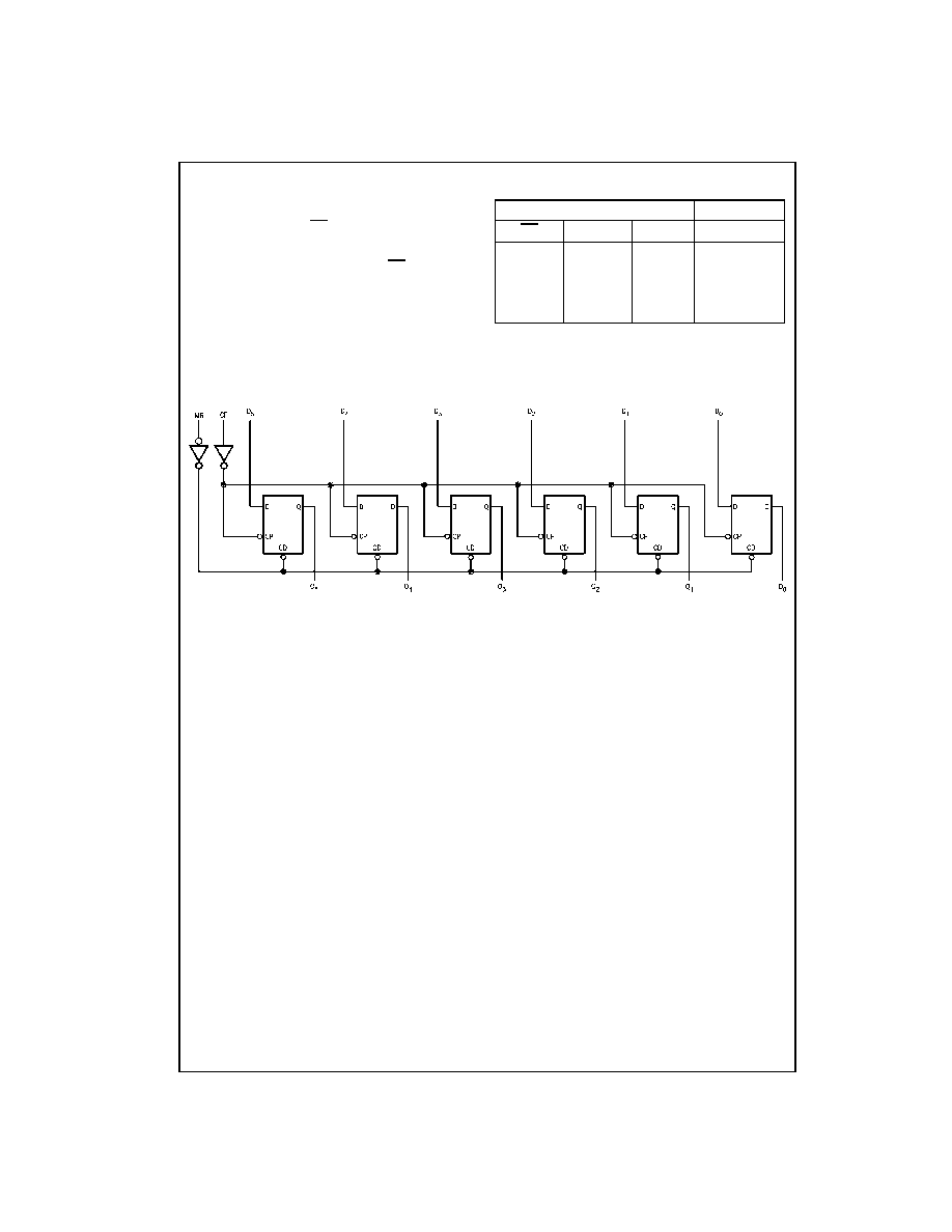
Functional Description
The AC/ACT174 consists of six edge-triggered D-type flip-
flops with individual D inputs and Q outputs. The Clock
(CP) and Master Reset (MR) are common to all flip-flops.
Each D input's state is transferred to the corresponding flip-
flop's output following the LOW-to-HIGH Clock (CP) transi-
tion. A LOW input to the Master Reset (MR) will force all
outputs LOW independent of Clock or Data inputs. The AC/
ACT174 is useful for applications where the true output
only is required and the Clock and Master Reset are com-
mon to all storage elements.
Truth Table
H
=
HIGH Voltage Level
L
=
LOW Voltage Level
=
LOW-to-HIGH Transition
X
=
Immaterial
Logic Diagram
Please note that this diagram is provided only for the understanding of logic operations and should not be used to estimate propagation delays.
Inputs
Output
MR
CP
D
Q
L
X
X
L
H
H
H
H
L
L
H
L
X
Q
3
www.fairchildsemi.com
74
A
C
17
4
∑
74ACT174
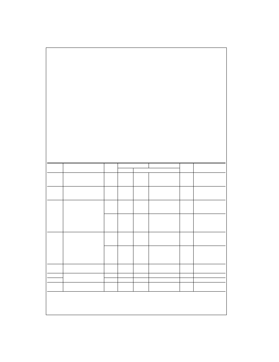
Absolute Maximum Ratings
(Note 1)
Recommended Operating
Conditions
Note 1: Absolute maximum ratings are those values beyond which damage
to the device may occur. The databook specifications should be met, with-
out exception, to ensure that the system design is reliable over its power
supply, temperature, and output/input loading variables. Fairchild does not
recommend operation of FACT
circuits outside databook specifications.
DC Electrical Characteristics for AC
Note 2: All outputs loaded; thresholds on input associated with output under test.
Note 3: Maximum test duration 2.0 ms, one output loaded at a time.
Note 4: I
IN
and I
CC
@ 3.0V are guaranteed to be less than or equal to the respective limit @ 5.5V V
CC
.
Supply Voltage (V
CC
)
-
0.5V to
+
7.0V
DC Input Diode Current (I
IK
)
V
I
=
-
0.5V
-
20 mA
V
I
=
V
CC
+
0.5V
+
20 mA
DC Input Voltage (V
I
)
-
0.5V to V
CC
+
0.5V
DC Output Diode Current (I
OK
)
V
O
=
-
0.5V
-
20 mA
V
=
V
CC
+
0.5V
+
20 mA
DC Output Voltage (V
O
)
-
0.5V to V
CC
+
0.5V
DC Output Source
or Sink Current (I
O
)
±
50 mA
DC V
CC
or Ground Current
per Output Pin (I
CC
or I
GND
)
±
50 mA
Storage Temperature (T
STG
)
-
65
∞
C to
+
150
∞
C
Junction Temperature (T
J
)
PDIP
140
∞
C
Supply Voltage (V
CC
)
AC
2.0V to 6.0V
ACT
4.5V to 5.5V
Input Voltage (V
I
)
0V to V
CC
Output Voltage (V
O
)
0V to V
CC
Operating Temperature (T
A
)
-
40
∞
C to
+
85
∞
C
Minimum Input Edge Rate (
V/
t)
AC Devices
V
IN
from 30% to 70% of V
CC
V
CC
@ 3.3V, 4.5V, 5.5V
125 mV/ns
Minimum Input Edge Rate (
V/
t)
ACT Devices
V
IN
from 0.8V to 2.0V
V
CC
@ 4.5V, 5.5V
125 mV/ns
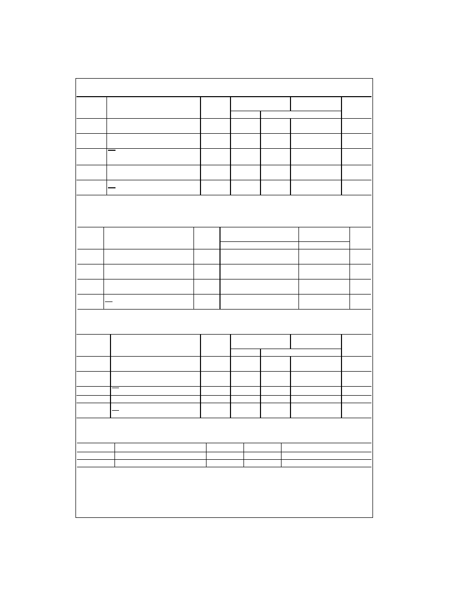
Symbol
Parameter
V
CC
T
A
=
+
25
∞
C T
A
=
-
40
∞
C to
+
85
∞
C
Units
Conditions
(V)
Typ
Guaranteed Limits
V
IH
Minimum HIGH Level
3.0
1.5
2.1
2.1
V
OUT
=
0.1V
Input Voltage
4.5
2.25
3.15
3.15
V
or V
CC
-
0.1V
5.5
2.75
3.85
3.85
V
IL
Maximum LOW Level
3.0
1.5
0.9
0.9
V
OUT
=
0.1V
Input Voltage
4.5
2.25
1.35
1.35
V
or V
CC
-
0.1V
5.5
2.75
1.65
1.65
V
OH
Minimum HIGH Level
3.0
2.99
2.9
2.9
Output Voltage
4.5
4.49
4.4
4.4
V
I
OUT
=
-
50
µ
A
5.5
5.49
5.4
5.4
V
IN
=
V
IL
or V
IH
3.0
2.56
2.46
I
OH
=
-
12 mA
4.5
3.86
3.76
V
I
OH
=
-
24 mA
5.5
4.86
4.76
I
OH
=
-
24 mA (Note 2)
V
OL
Maximum LOW Level
3.0
0.002
0.1
0.1
Output Voltage
4.5
0.001
0.1
0.1
V
I
OUT
=
50
µ
A
5.5
0.001
0.1
0.1
V
IN
=
V
IL
or V
IH
3.0
0.36
0.44
I
OL
= 12 mA
4.5
0.36
0.44
V
I
OL
= 24 mA
5.5
0.36
0.44
I
OL
= 24 mA (Note 2)
I
IN
Maximum Input
5.5
±
0.1
±
1.0
µ
A
V
I
=
V
CC
(Note 4)
Leakage Current
or GND
I
OLD
Minimum Dynamic
5.5
75
mA
V
OLD
=
1.65V Max
I
OHD
Output Current (Note 3)
5.5
-
75
mA
V
OHD
=
3.85V Min
I
CC
Maximum Quiescent
5.5
4.0
40.0
µ
A
V
IN
=
V
CC
(Note 4)
Supply Current
or GND
www.fairchildsemi.com
4
74AC174
∑
74ACT174
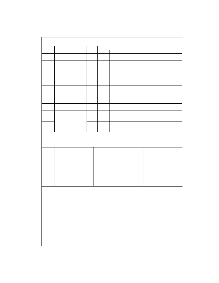
DC Electrical Characteristics for ACT
Note 5: All outputs loaded; thresholds on input associated with output under test.
Note 6: Maximum test duration 2.0 ms, one output loaded at a time.
AC Electrical Characteristics for AC
Note 7: Voltage Range 3.3 is 3.3V
±
0.3V
Voltage Range 5.0 is 5.0V
±
0.5V
Symbol
Parameter
V
CC
T
A
=
+
25
∞
C
T
A
=
-
40
∞
C to
+
85
∞
C
Units
Conditions
(V)
Typ
Guaranteed Limits
V
IH
Minimum HIGH Level
4.5
1.5
2.0
2.0
V
V
OUT
=
0.1V
Input Voltage
5.5
1.5
2.0
2.0
or V
CC
-
0.1V
V
IL
Maximum LOW Level
4.5
1.5
0.8
0.8
V
V
OUT
=
0.1V
Input Voltage
5.5
1.5
0.8
0.8
or V
CC
-
0.1V
V
OH
Minimum HIGH Level
4.5
4.49
4.4
4.4
V
I
OUT
=
-
50
µ
A
Output Voltage
5.5
5.49
5.4
5.4
V
IN
=
V
IL
or V
IH
4.5
3.86
3.76
V
I
OH
=
-
24 mA
5.5
4.86
4.76
I
OH
=
-
24 mA (Note 5)
V
OL
Maximum LOW Level
4.5
0.001
0.1
0.1
V
I
OUT
=
50
µ
A
Output Voltage
5.5
0.001
0.1
0.1
V
IN
=
V
IL
or V
IH
4.5
0.36
0.44
V
I
OL
= 24 mA
5.5
0.36
0.44
I
OL
= 24 mA (Note 5)
I
IN
Maximum Input
5.5
±
0.1
±
1.0
µ
A
V
I
=
V
CC
, GND
Leakage Current
I
CCT
Maximum
5.5
0.6
1.5
mA
V
I
=
V
CC
-
2.1V
I
CC
/Input
I
OLD
Minimum Dynamic
5.5
75
mA
V
OLD
=
1.65V Max
I
OHD
Output Current (Note 6)
5.5
-
75
mA
V
OHD
=
3.85V Min
I
CC
Maximum Quiescent
5.5
4.0
40.0
µ
A
V
IN
=
V
CC
Supply Current
or GND
Symbol
Parameter
V
CC
(V)
(Note 7)
T
A
=
+
25
∞
C
C
L
=
50 pF
T
A
=
-
40
∞
C to
+
85
∞
C
C
L
=
50 pF
Units
Min
Typ
Max
Min
Max
f
MAX
Maximum Clock
3.3
90
100
70
MHz
Frequency
5.0
100
125
100
t
PLH
Propagation Delay
3.3
2.0
9.0
11.5
1.5
12.5
ns
CP to Q
n
5.0
1.5
6.0
8.5
1.0
9.5
t
PHL
Propagation Delay
3.3
2.0
8.5
11.0
1.5
12.0
ns
CP to Q
n
5.0
1.5
6.0
8.0
1.0
9.0
t
PHL
Propagation Delay
3.3
2.5
9.0
11.5
2.0
12.5
ns
MR to Q
n
5.0
1.5
7.0
9.0
1.5
10.5
5
www.fairchildsemi.com
74
A
C
17
4
∑
74ACT174
AC Operating Requirements for AC
Note 8: Voltage Range 3.3 is 3.3V
±
0.3V
Voltage Range 5.0 is 5.0V
±
0.5V
AC Electrical Characteristics for ACT
Note 9: Voltage Range 5.0 is 5.0V
±
0.5V
AC Operating Requirements for ACT
Note 10: Voltage Range 5.0 is 5.0V
±
0.5V
Capacitance
Symbol
Parameter
V
CC
(V)
(Note 8)
T
A
=
+
25
∞
C
C
L
=
50 pF
T
A
=
-
40
∞
C to
+
85
∞
C
C
L
=
50 pF
Units
Typ
Guaranteed Minimum
t
S
Setup Time, HIGH or LOW
3.3
2.5
6.5
7.0
ns
D
n
to CP
5.0
2.0
5.0
5.5
t
H
Hold Time, HIGH or LOW
3.3
1.0
3.0
3.0
ns
D
n
to CP
5.0
0.5
3.0
3.0
t
W
MR Pulse Width, LOW
3.3
1.0
5.5
7.0
ns
5.0
1.0
5.0
5.0
t
W
CP Pulse Width
3.3
1.0
5.5
7.0
ns
5.0
1.0
5.0
5.0
t
REC
Recovery Time
3.3
0
2.5
2.5
ns
MR to CP
5.0
0
2.0
2.0
Symbol
Parameter
V
CC
(V)
(Note 9)
T
A
=
+
25
∞
C
C
L
=
50 pF
T
A
=
-
40
∞
C to
+
85
∞
C
C
L
=
50 pF
Units
Min
Typ
Max
Min
Max
f
MAX
Maximum Clock
5.0
165
200
140
MHz
Frequency
t
PLH
Propagation Delay
5.0
1.5
7.0
10.5
1.5
11.5
ns
CP to Q
n
t
PHL
Propagation Delay
5.0
1.5
7.0
10.5
1.5
11.5
ns
CP to Q
n
t
PHL
Propagation Delay
5.0
1.5
6.5
9.5
1.5
11.0
ns
MR to Q
n
Symbol
Parameter
V
CC
(V)
(Note 10)
T
A
=
+
25
∞
C
C
L
=
50 pF
T
A
=
-
40
∞
C to
+
85
∞
C
C
L
=
50 pF
Units
Typ
Guaranteed Minimum
t
S
Setup Time, HIGH or LOW
5.0
0.5
1.5
1.5
ns
D
n
to CP
t
H
Hold Time, HIGH or LOW
5.0
1.0
2.0
2.0
ns
D
n
to CP
t
W
MR Pulse Width, LOW
5.0
1.5
3.0
3.5
ns
t
W
CP Pulse Width, HIGH or LOW
5.0
1.5
3.0
3.5
ns
t
rec
Recovery Time
5.0
-
1.0
0.5
0.5
ns
MR to CP
Symbol
Parameter
Typ
Units
Conditions
C
IN
Input Capacitance
4.5
pF
V
CC
=
OPEN
C
PD
Power Dissipation Capacitance
85.0
pF
V
CC
=
5.0V