© 1999 Fairchild Semiconductor Corporation
DS009941
www.fairchildsemi.com
November 1988
Revised November 1999
7
4
AC
2
40 ∑
74ACT240
O
c
t
a
l
Buf
f
er
/Li
n
e Dr
ive
r
wi
th
3-ST
A
T
E Out
puts
74AC240 ∑ 74ACT240
Octal Buffer/Line Driver with 3-STATE Outputs
General Description
The AC/ACT240 is an octal buffer and line driver designed
to be employed as a memory address driver, clock driver
and bus oriented transmitter or receiver which provides
improved PC board density.
Features
s
I
CC
and I
OZ
reduced by 50%
s
Inverting 3-STATE outputs drive bus lines or buffer
memory address registers
s
Outputs source/sink 24 mA
s
ACT240 has TTL-compatible inputs
Ordering Code:
Device also available in Tape and Reel. Specify by appending suffix letter "X" to the ordering code.
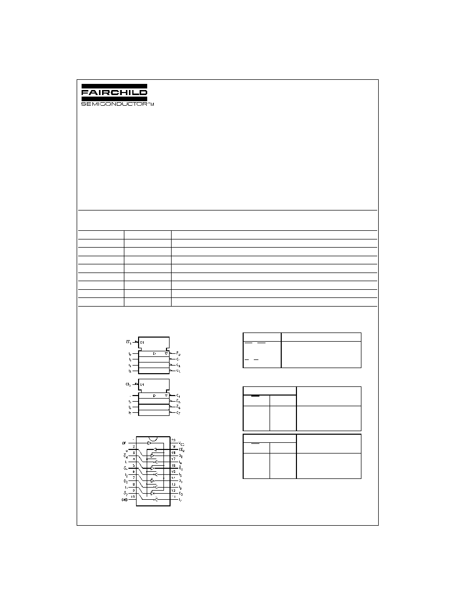
Logic Symbol
IEEE/IEC
Connection Diagram
Pin Descriptions
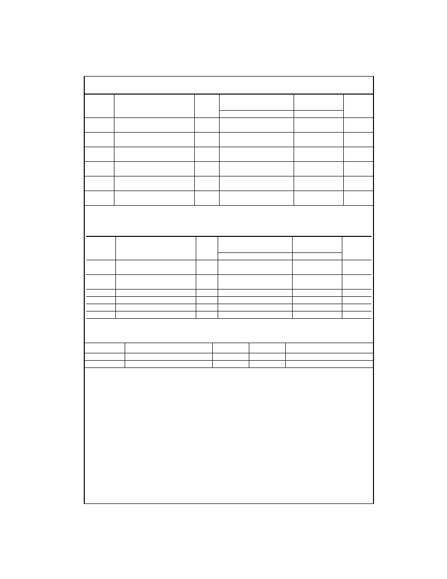
Truth Tables
H
=
HIGH Voltage Level
L
=
LOW Voltage Level
X
=
Immaterial
Z
=
High Impedance
FACT
is a trademark of Fairchild Semiconductor Corporation.
Order Number
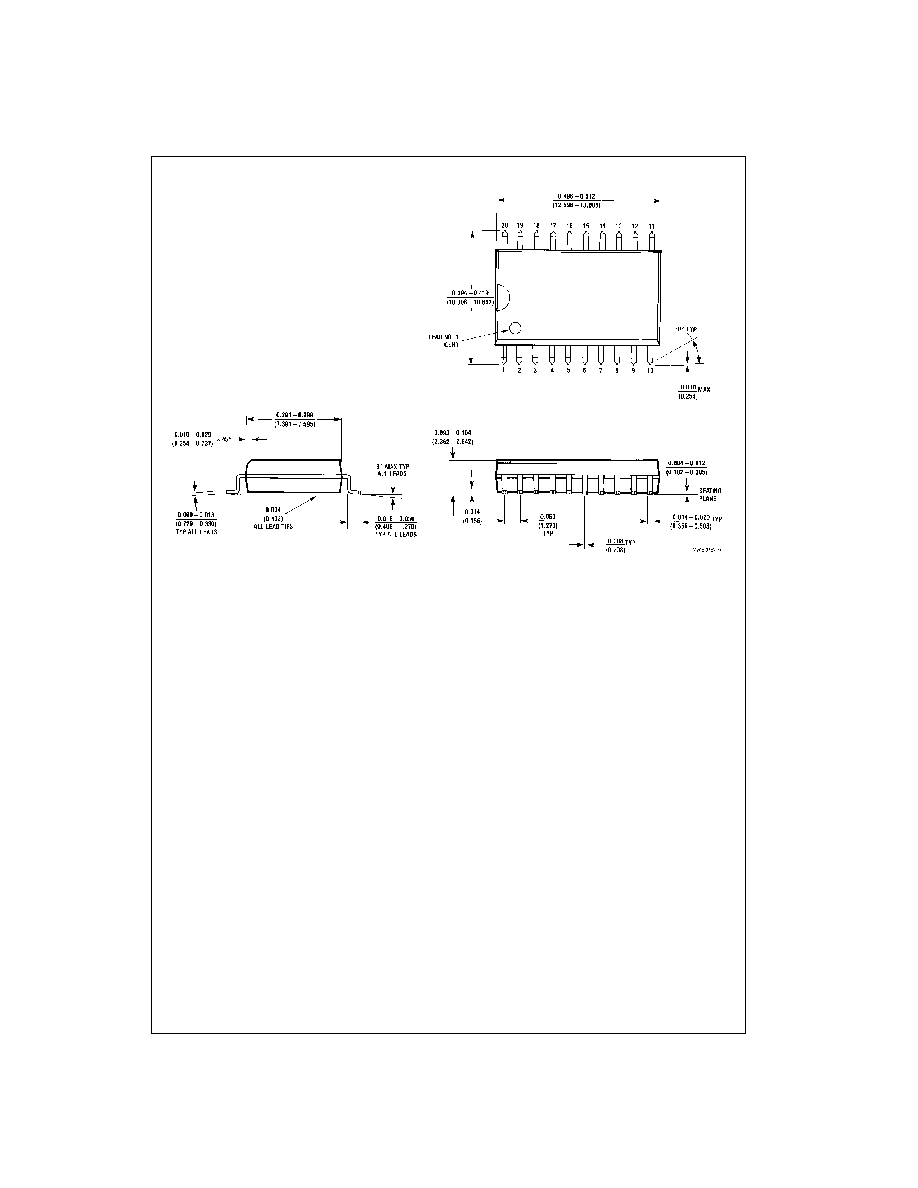
Package Number
Package Description
74AC240SC
M20B
20-Lead Small Outline Integrated Circuit (SOIC), JEDEC MS-013, 0.300" Wide Body
74AC240SJ
M20D
20-Lead Small Outline Package (SOP), EIAJ TYPE II, 5.3mm Wide
74AC240MTC
MTC20
20-Lead Thin Shrink Small Outline Package (TSSOP), JEDEC MO-153,4.4mm Wide
74AC240PC
N20A
20-Lead Plastic Dual-In-Line Package (PDIP), JEDEC MS-001, 0.300" Wide
74ACT240SC
M20B
20-Lead Small Outline Integrated Circuit (SOIC), JEDEC MS-013, 0.300" Wide Body
74ACT240SJ
M20D
20-Lead Small Outline Package (SOP), EIAJ TYPE II, 5.3mm Wide
74ACT240MTC
MTC20
20-Lead Thin Shrink Small Outline Package (TSSOP), JEDEC MO-153,4.4mm Wide
74ACT240PC
N20A
20-Lead Plastic Dual-In-Line Package (PDIP), JEDEC MS-001, 0.300" Wide
Pin Names
Description
OE
1
, OE
2
3-STATE Output Enable Inputs
I
0
≠I
7
Inputs
O
0
≠O
7
Outputs
Inputs
Outputs
OE
1
I
n
(Pins 12, 14, 16, 18)
L
L
H
L
H
L
H
X
Z
Inputs
Outputs
OE
2
I
n
(Pins 3, 5, 7, 9)
L
L
H
L
H
L
H
X
Z
www.fairchildsemi.com
2
74AC240
∑
74ACT240
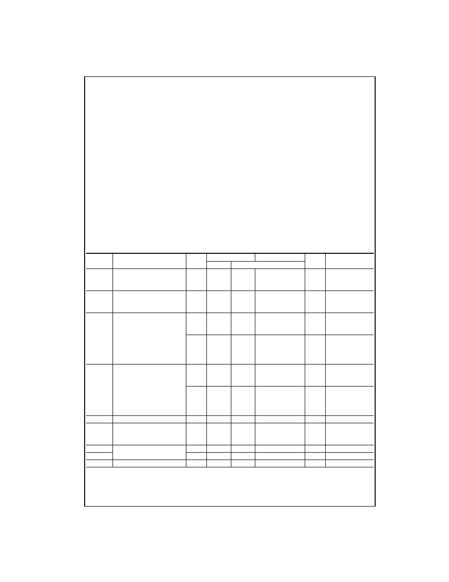
Absolute Maximum Ratings
(Note 1)
Recommended Operating
Conditions
Note 1: Absolute maximum ratings are those values beyond which damage
to the device may occur. The databook specifications should be met, with-
out exception, to ensure that the system design is reliable over its power
supply, temperature, and output/input loading variables. Fairchild does not
recommend operation of FACT
circuits outside databook specifications.
DC Electrical Characteristics for AC
Note 2: All outputs loaded; thresholds on input associated with output under test.
Note 3: Maximum test duration 2.0 ms, one output loaded at a time.
Note 4: I
IN
and I
CC
@ 3.0V are guaranteed to be less than or equal to the respective limit @ 5.5V V
CC
.
Supply Voltage (V
CC
)
-
0.5V to
+
7.0V
DC Input Diode Current (I
IK
)
V
I
=
-
0.5V
-
20 mA
V
I
=
V
CC
+
0.5V
+
20 mA
DC Input Voltage (V
I
)
-
0.5V to V
CC
+
0.5V
DC Output Diode Current (I
OK
)
V
O
=
-
0.5V
-
20 mA
V
O
=
V
CC
+
0.5V
+
20 mA
DC Output Voltage (V
O
)
-
0.5V to V
CC
+
0.5V
DC Output Source
or Sink Current (I
O
)
±
50 mA
DC V
CC
or Ground Current
per Output Pin (I
CC
or I
GND
)
±
50 mA
Storage Temperature (T
STG
)
-
65
∞
C to
+
150
∞
C
Junction Temperature (T
J
)
PDIP
140
∞
C
Supply Voltage (V
CC
)
AC
2.0V to 6.0V
ACT
4.5V to 5.5V
Input Voltage (V
I
)
0V to V
CC
Output Voltage (V
O
)
0V to V
CC
Operating Temperature (T
A
)
-
40
∞
C to
+
85
∞
C
Minimum Input Edge Rate (
V/
t)
AC Devices
V
IN
from 30% to 70% of V
CC
V
CC
@ 3.3V, 4.5V, 5.5V
125 mV/ns
Minimum Input Edge Rate (
V/
t)
ACT Devices
V
IN
from 0.8V to 2.0V
V
CC
@ 4.5V, 5.5V
125 mV/ns
Symbol
Parameter
V
CC
(V)
T
A
=
+
25
∞
C
T
A
=
-
40
∞
C to
+
85
∞
C
Units
Conditions
Typ
Guaranteed Limits
V
IH
Minimum HIGH Level
3.0
1.5
2.1
2.1
V
OUT
=
0.1V
Input Voltage
4.5
2.25
3.15
3.15
V
or V
CC
-
0.1V
5.5
2.75
3.85
3.85
V
IL
Maximum LOW Level
3.0
1.5
0.9
0.9
V
OUT
=
0.1V
Input Voltage
4.5
2.25
1.35
1.35
V
or V
CC
-
0.1V
5.5
2.75
1.65
1.65
V
OH
Minimum HIGH Level
3.0
2.99
2.9
2.9
Output Voltage
4.5
4.49
4.4
4.4
V
I
OUT
=
-
50
µ
A
5.5
5.49
5.4
5.4
V
IN
=
V
IL
or V
IH
3.0
2.56
2.46
I
OH
=
-
12 mA
4.5
3.86
3.76
V
I
OH
=
-
24 mA
5.5
4.86
4.76
I
OH
=
-
24 mA (Note 2)
V
OL
Maximum LOW Level
3.0
0.002
0.1
0.1
Output Voltage
4.5
0.001
0.1
0.1
V
I
OUT
=
50
µ
A
5.5
0.001
0.1
0.1
V
IN
=
V
IL
or V
IH
3.0
0.36
0.44
I
OL
=
12 mA
4.5
0.36
0.44
V
I
OL
=
24 mA
5.5
0.36
0.44
I
OL
=
24 mA (Note 2)
I
IN
(Note 4)
Maximum Input Leakage Current
5.5
±
0.1
±
1.0
µ
A
V
I
=
V
CC
, GND
I
OZ
Maximum 3-STATE
V
I
(OE)
=
V
IL
, V
IH
Leakage Current
5.5
±
0.25
±
2.5
µ
A
V
I
=
V
CC
, GND
V
O
=
V
CC
, GND
I
OLD
Minimum Dynamic
5.5
75
mA
V
OLD
=
1.65V Max
I
OHD
Output Current (Note 3)
5.5
-
75
mA
V
OHD
=
3.85V Min
I
CC
(Note 4) Maximum Quiescent Supply Current
5.5
4.0
40.0
µ
A
V
IN
=
V
CC
or GND
3
www.fairchildsemi.com
74
A
C
24
0
∑
74ACT240
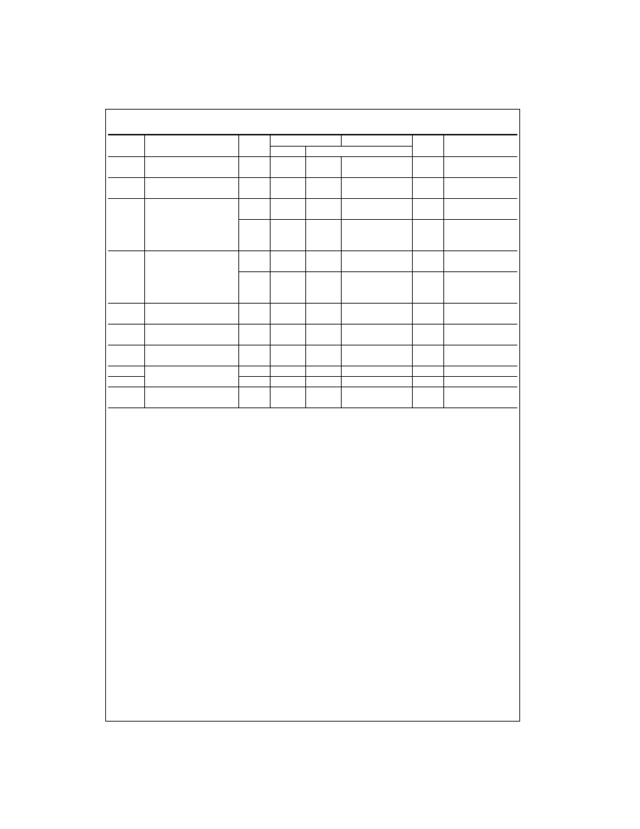
DC Electrical Characteristics for ACT
Note 5: All outputs loaded; thresholds on input associated with output under test.
Note 6: Maximum test duration 2.0 ms, one output loaded at a time.
Symbol
Parameter
V
CC
T
A
=
+
25
∞
C
T
A
=
-
40
∞
C to
+
85
∞
C
Units
Conditions
(V)
Typ
Guaranteed Limits
V
IH
Minimum HIGH Level
4.5
1.5
2.0
2.0
V
V
OUT
=
0.1V
Input Voltage
5.5
1.5
2.0
2.0
or V
CC
-
0.1V
V
IL
Maximum LOW Level
4.5
1.5
0.8
0.8
V
V
OUT
=
0.1V
Input Voltage
5.5
1.5
0.8
0.8
or V
CC
-
0.1V
V
OH
Minimum HIGH Level
4.5
4.49
4.4
4.4
V
I
OUT
=
-
50
µ
A
Output Voltage
5.5
5.49
5.4
5.4
V
IN
=
V
IL
or V
IH
4.5
3.86
3.76
V
I
OH
=
-
24 mA
5.5
4.86
4.76
I
OH
=
-
24 mA (Note 5)
V
OL
Maximum LOW Level
4.5
0.001
0.1
0.1
V
I
OUT
=
50
µ
A
Output Voltage
5.5
0.001
0.1
0.1
V
IN
=
V
IL
or V
IH
4.5
0.36
0.44
V
I
OL
=
24 mA
5.5
0.36
0.44
I
OL
=
24 mA (Note 5)
I
IN
Maximum Input
5.5
±
0.1
±
1.0
µ
A
V
I
=
V
CC
, GND
Leakage Current
I
OZ
Maximum 3-STATE
5.5
±
0.25
±
2.5
µ
A
V
I
=
V
IL
, V
IH
Leakage Current
V
O
=
V
CC
, GND
I
CCT
Maximum
5.5
0.6
1.5
mA
V
I
=
V
CC
-
2.1V
I
CC
/Input
I
OLD
Minimum Dynamic
5.5
75
mA
V
OLD
=
1.65V Max
I
OHD
Output Current (Note 6)
5.5
-
75
mA
V
OHD
=
3.85V Min
I
CC
Maximum Quiescent
5.5
4.0
40.0
µ
A
V
IN
=
V
CC
Supply Current
or GND
www.fairchildsemi.com
4
74AC240
∑
74ACT240
AC Electrical Characteristics
Note 7: Voltage Range 3.3 is 3.3V
±
0.3V
Voltage Range 5.0 is 5.0V
±
0.5V
AC Electrical Characteristics
Note 8: Voltage Range 5.0 is 5.0V
±
0.5V
Capacitance
V
CC
T
A
=
+
25
∞
C
T
A
=
-
40
∞
C to
+
85
∞
C
Symbol
Parameter
(V)
C
L
=
50 pF
C
L
=
50 pF
Units
(Note 7)
Min
Typ
Max
Min
Max
t
PLH
Propagation Delay
3.3
1.5
6.0
8.0
1.0
9.0
ns
Data to Output
5.0
1.5
4.5
6.5
1.0
7.0
t
PHL
Propagation Delay
3.3
1.5
5.5
8.0
1.0
8.5
ns
Data to Output
5.0
1.5
4.5
6.0
1.0
6.5
t
PZH
Output Enable Time
3.3
1.5
6.0
10.5
1.0
11.0
ns
5.0
1.5
5.0
7.0
1.0
8.0
t
PZL
Output Enable Time
3.3
1.5
7.0
10.0
1.0
11.0
ns
5.0
1.5
5.5
8.0
1.0
8.5
t
PHZ
Output Disable Time
3.3
1.5
7.0
10.0
1.0
10.5
ns
5.0
1.5
6.5
9.0
1.0
9.5
t
PLZ
Output Disable Time
3.3
1.5
7.5
10.5
1.0
11.5
ns
5.0
1.5
6.5
9.0
1.0
9.5
V
CC
T
A
=
+
25
∞
C
T
A
=
-
40
∞
C to
+
85
∞
C
Symbol
Parameter
(V)
C
L
=
50 pF
C
L
=
50 pF
Units
(Note 8)
Min
Typ
Max
Min
Max
t
PLH
Propagation Delay
5.0
1.5
6.0
8.5
1.5
9.5
ns
Data to Output
t
PHL
Propagation Delay
5.0
1.5
5.5
7.5
1.5
8.5
ns
Data to Output
t
PZH
Output Enable Time
5.0
1.5
7.0
8.5
1.0
9.5
ns
t
PZL
Output Enable Time
5.0
2.0
7.0
9.5
1.5
10.5
ns
t
PHZ
Output Disable Time
5.0
2.0
8.0
9.5
2.0
10.5
ns
t
PLZ
Output Disable Time
5.0
2.5
6.5
10.0
2.0
10.5
ns
Symbol
Parameter
Typ
Units
Conditions
C
IN
Input Capacitance
4.5
pF
V
CC
=
OPEN
C
PD
Power Dissipation Capacitance
45.0
pF
V
CC
=
5.0V