© 1999 Fairchild Semiconductor Corporation
DS011683
www.fairchildsemi.com
June 1996
Revised November 1999
7
4
AC
T1
284 I
EEE 128
4 T
r
anscei
ver
74ACT1284
IEEE 1284 Transceiver
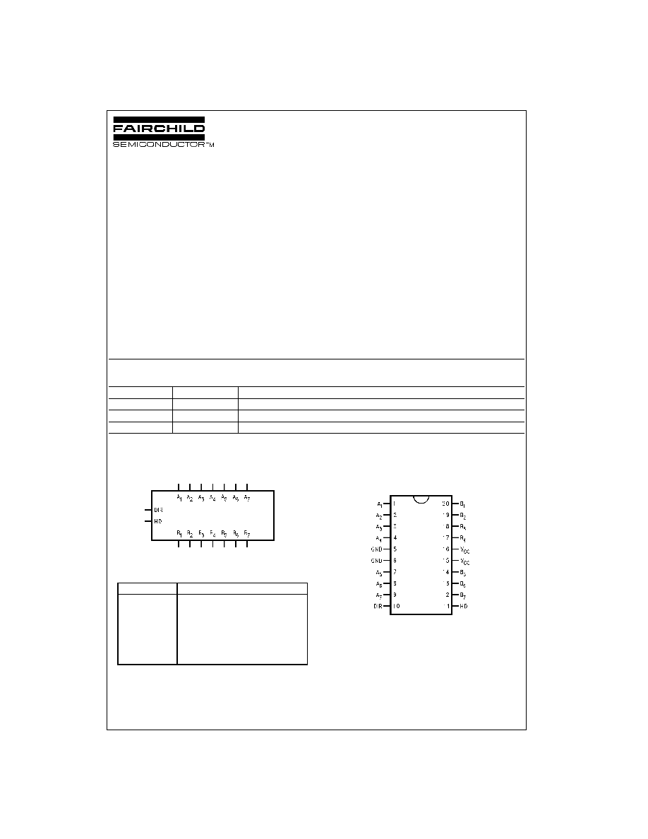
General Description
The 74ACT1284 contains four non-inverting bidirectional
buffers and three non-inverting buffers with open Drain out-
puts and high drive capability on the B Ports. It is intended
to provide a standard signaling method for a bi-direction
parallel peripheral in an Extended Capabilities Port mode
(ECP).
The HD (active HIGH) input pin enables the B Ports to
switch from open Drain to a high drive totem pole output,
capable of sourcing 14 mA on all seven buffers. The DIR
input determines the direction of data flow on the bidirec-
tional buffers. DIR (active HIGH) enables data flow from A
Ports to B Ports. DIR (active LOW) enables data flow from
B Ports to A Ports.
Features
s
TTL-compatible inputs
s
A Ports have standard 4 mA totem pole outputs
s
Typical input hysteresis of 0.5V
s
B Port high drive source/sink capability of 14 mA
s
Bidirectional non-inverting buffers
s
Supports IEEE P1284 Level 1 and Level 2 signaling
standards for bidirectional parallel communications
between personal computers and printing peripherals
s
B Port outputs in High Impedance mode during power
down
s
Guaranteed 4000V minimum ESD protection
Ordering Code:
Device also available in Tape and Reel. Specify by appending suffix letter "X" to the ordering code.
Logic Symbol
Pin Descriptions
Connection Diagram
FACT
is a trademark of Fairchild Semiconductor Corporation.
Order Number
Package Number
Package Description
74ACT1284SC
M20B
20-Lead Small Outline Integrated Circuit (SOIC), JEDEC MS-013, 0.300 Wide
74ACT1284MSA
MSA20
20-Lead Shrink Small Outline Package (SSOP), EIAJ TYPE II, 5.3mm Wide
74ACT1284MTC
MTC20
20-Lead Thin Shrink Small Outline Package (TSSOP), JEDEC MO-153, 4.4mm Wide
Pin Names
Description
HD
High Drive Enable input (Active HIGH)
DIR
Direction Control Input
A
1
- A
4
Side A Inputs or Outputs
B
1
- B
4
Side B Inputs or Outputs
A
5
- A
7
Side A Inputs
B
5
- B
7
Side B Outputs
3
www.fairchildsemi.com
7
4
AC
T1
284
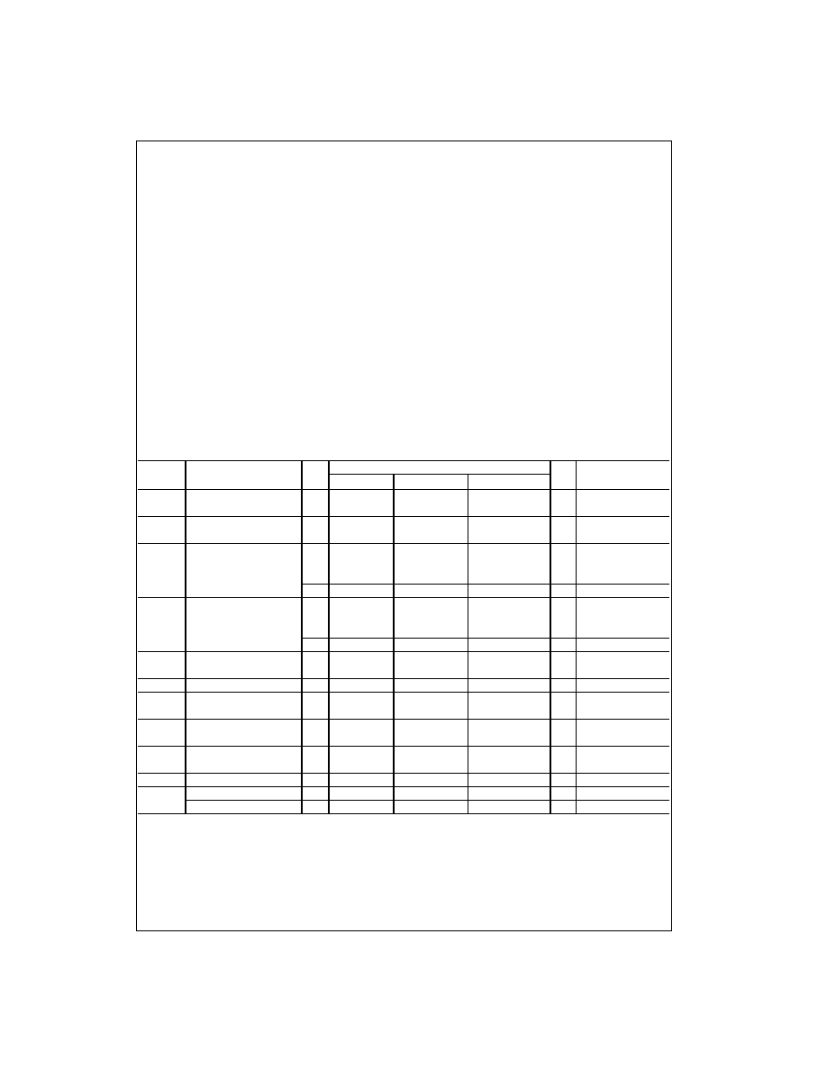
Absolute Maximum Ratings
(Note 3)
(Note 4)
Recommended Operating
Conditions
Note 3: Absolute maximum ratings are those values beyond which damage
to the device may occur. The databook specifications should be met, with-
out exception, to ensure that the system design is reliable over its power
supply, temperature, and output/input loading variables. Fairchild does not
recommend operation of FACT
circuits outside databook specifications.
Note 4: Either voltage limit or current limit is sufficient to protect inputs.
DC Electrical Characteristics
Note 5: All outputs loaded; thresholds on input associated with output under test.
Note 6: This parameter is guaranteed but not tested, characterized only: RD is the measure of the B-Side output impedance with the output in the HIGH
state.
Supply Voltage (V
CC
)
-
0.5V to
+
7.0V
DC Input Diode Current (I
IK
)
V
I
=
-
0.5V
-
20 mA
V
I
=
V
CC
+
0.5V
+
20 mA
DC Input Voltage (V
I
) A Side
-
0.5V to V
CC
+
0.5V
DC Input Voltage (V
I
) B Side
-
2V to
+
7V
DC Output Diode Current (I
OK
)
V
O
=
-
0.5V
-
20 mA
V
O
=
V
CC
+
0.5V
+
20 mA
DC Output Voltage (V
O
) A Side
-
0.5V to V
CC
+
0.5V
DC Output Voltage (V
O
) B Side
-
2V to
+
7V
DC Output Source
or Sink Current (I
O
)
±
50 mA
DC V
CC
or Ground Current
per Output Pin (I
CC
or I
GND
)
±
50 mA
Storage Temperature (T
STG
)
-
65
∞
C to
+
150
∞
C
Supply Voltage (V
CC
)
4.7V to 5.5V
Input Voltage (V
I
)
0V to V
CC
Output Voltage (V
O
)
0V to V
CC
Operating Temperature (T
A
)
-
40
∞
C to
+
85
∞
C
Symbol
Parameter
V
CC
(V)
Guaranteed Limits
Units
Conditions
T
A
=
+
25
∞
C
T
A
=
0
∞
C to
+
70
∞
C T
A
=
-
40
∞
C to
+
85
∞
C
V
IH
Minimum HIGH Level
4.7
2.0
2.0
2.0
V
Recognized
Input Voltage
5.5
2.0
2.0
2.0
High Signal
V
IL
Maximum LOW Level
4.7
0.8
0.8
0.8
V
Recognized
Input Voltage
5.5
0.8
0.8
0.8
Low Signal
V
OH
Minimum HIGH Level
4.7
4.5
4.5
4.5
I
OUT
=
-
50
µ
A (An)
Output Voltage
V
V
IN
=
V
IL
or V
IH
(Note 5)
4.7
3.7
3.7
3.7
I
OH
=
-
4 mA (A
n
)
4.7
2.4
2.4
2.4
V
I
OH
=
-
14 mA (B
n
)
V
OL
Maximum LOW Level
4.7
0.2
0.2
0.2
I
OUT
=
50
µ
A (An)
Output Voltage
V
V
IN
=
V
IL
or V
IH
(Note 5)
4.7
0.4
0.4
0.4
I
OH
=
4 mA (A
n
)
V
I
OH
=
14 mA (B
n
)
I
IN
Maximum Input
5.5
±
0.1
±
1.0
µ
A
V
I
=
V
CC
, GND
Leakage Current
(DIR, A5, A6, A7, HD)
I
CCT
Maximum I
CC
/Input
5.5
1.5
1.5
mA
V
I
=
V
CC
-
2.1V
I
CC
Maximum Quiescent
5.5
400
400
500
µ
A
V
IN
=
V
CC
or GND
Supply Current
I
OZ
Maximum Output
5.5
±
20
±
20
±
20
µ
A
V
O
=
V
CC
, GND
Leakage Current
I
OFF
Maximum B-Side Power Down
0.0
100
100
100
µ
A
V
OUT
=
5.25V
Leakage Current
VT
Input Hysteresis
5.0
0.4
0.4
0.35
V
V
T
+
-
V
T
-
R
D
Maximum Output Impedance
5.0
22
22
24
B
n
(Note 6)
Minimum Output Impedance
5.0
8
8
6
B
n
(Note 6)
www.fairchildsemi.com
4
74ACT1284
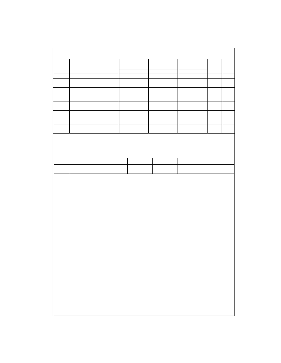
AC Electrical Characteristics
Note 7: Open Drain
Note 8: This parameter is guaranteed but not tested, characterized only.
Note: Pulse Generator for all pulses; Rate
1.0 MHz; AO
50
; t
f
2.5 ns, t
r
2.5 ns.
Capacitance
Symbol
Parameter
T
A
=
+
25
∞
C
T
A
=
0
∞
C to
+
70
∞
C
T
A
=
-
40
∞
C to
+
85
∞
C
Units
Figure
Number
V
CC
=
4.7V
-
5.5V
V
CC
=
4.7V
-
5.5V
V
CC
=
4.7V
-
5.5V
Min
Max
Min
Max
Min
Max
t
PHL
A
1
- A
7
to B
1
- B
7
2.0
20.0
2.0
20.0
2.0
24.0
ns
Figure 1
t
PLH
A
1
- A
7
to B
1
- B
7
2.0
20.0
2.0
20.0
2.0
24.0
ns
Figure 2
t
PHL
B
1
- B
4
to A
1
- A
4
2.0
20.0
2.0
20.0
2.0
24.0
ns
Figure 3
t
PLH
B
1
- B
4
to A
1
- A
4
2.0
20.0
2.0
20.0
2.0
24.0
ns
Figure 3
t
pEnable
Output
Enable
Time
2.0
20.0
2.0
20.0
2.0
24.0
ns
Figure 2
HD to B
1
- B
7
t
pDisable
Output Disable Time
2.0
20.0
2.0
20.0
2.0
24.0
ns
Figure 2
HD to B
1
- B
7
t
SKEW
Output Slew Rate
0.05
0.40
0.05
0.40
0.05
0.40
V/ns
Figure 1
t
PLH
B
1
- B
7
Figure 2
t
PHL
t
r
, t
f
t
RISE
and t
FALL
120
120
120
ns
Figure 4
B
1
- B
7
(Note 7)
(Note 8)
Symbol
Parameter
Typ
Units
Conditions
C
IN
Input Capacitance
4.0
pF
V
CC
=
OPEN (HD, DIR A
5
- A
7
)
C
I/O
I/O Pin Capacitance
12.0
pF
V
CC
=
5.0V

5
www.fairchildsemi.com
7
4
AC
T1
284
AC Loading and Waveforms
t
SLEW
measures between 10% to 90% on the t
PHL
Transition
FIGURE 1. A to B Direction Test Load and Waveforms
t
SLEW
measures between 10% to 90% on the t
PLH
Transition
FIGURE 2. B Output Test Load and Waveforms
FIGURE 3. B to A Direction Test Load and Waveforms for Outputs A
1
- A
4
FIGURE 4. A to B Direction Test Load and Waveforms for Open Drain B
1
- B
7
