© 2000 Fairchild Semiconductor Corporation
DS009954
www.fairchildsemi.com
November 1988
Revised August 2000
7
4
AC
2
73 ∑
74ACT273
O
c
t
a
l
D-
T
y
pe Fl
ip-
F
l
o
p
74AC273 ∑ 74ACT273
Octal D-Type Flip-Flop
General Description
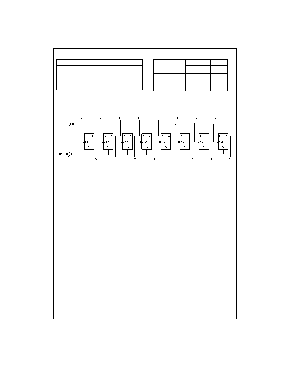
The AC273 and ACT273 have eight edge-triggered D-type
flip-flops with individual D-type inputs and Q outputs. The
common buffered Clock (CP) and Master Reset (MR) input
load and reset (clear) all flip-flops simultaneously.
The register is fully edge-triggered. The state of each D-
type input, one setup time before the LOW-to-HIGH clock
transition, is transferred to the corresponding flip-flop's Q
output.
All outputs will be forced LOW independently of Clock or
Data inputs by a LOW voltage level on the MR input. The
device is useful for applications where the true output only
is required and the Clock and Master Reset are common to
all storage elements.
Features
s
Ideal buffer for microprocessor or memory
s
Eight edge-triggered D-type flip-flops
s
Buffered common clock
s
Buffered, asynchronous master reset
s
See 377 for clock enable version
s
See 373 for transparent latch version
s
See 374 for 3-STATE version
s
Outputs source/sink 24 mA
s
74ACT273 has TTL-compatible inputs
Ordering Code:
Device also available in Tape and Reel. Specify by appending suffix letter "X" to the ordering code.
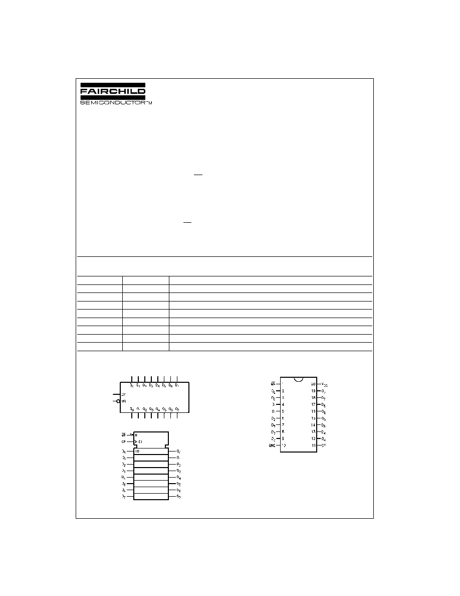
Logic Symbols
IEEE/IEC
Connection Diagram
FACT
is a trademark of Fairchild Semiconductor Corporation.
Order Number
Package Number
Package Description
74AC273SC
M20B
20-Lead Small Outline Integrated Circuit (SOIC), JEDEC MS-013, 0.300 Wide
74AC273SJ
M20D
20-Lead Small Outline Package (SOP), EIAJ TYPE II, 5.3mm Wide
74AC273MTC
MTC20
20-Lead Thin Shrink Small Outline Package (TSSOP), JEDEC MO-153, 4.4mm Wide
74AC273PC
N20A
20-Lead Plastic Dual-In-Line Package (PDIP), JEDEC MS-001, 0.300 Wide
74ACT273SC
M20B
20-Lead Small Outline Integrated Circuit (SOIC), JEDEC MS-013, 0.300 Wide
74ACT273SJ
M20D
20-Lead Small Outline Package (SOP), EIAJ TYPE II, 5.3mm Wide
74ACT273MTC
MTC20
20-Lead Thin Shrink Small Outline Package (TSSOP), JEDEC MO-153, 4.4mm Wide
74ACT273PC
N20A
20-Lead Plastic Dual-In-Line Package (PDIP), JEDEC MS-001, 0.300 Wide
3
www.fairchildsemi.com
74
A
C
27
3
∑
74ACT273
Absolute Maximum Ratings
(Note 1)
Recommended Operating
Conditions
Note 1: Absolute maximum ratings are those values beyond which damage
to the device may occur. The databook specifications should be met, with-
out exception, to ensure that the system design is reliable over its power
supply, temperature, and output/input loading variables. Fairchild does not
recommend operation of FACT
circuits outside databook specifications.
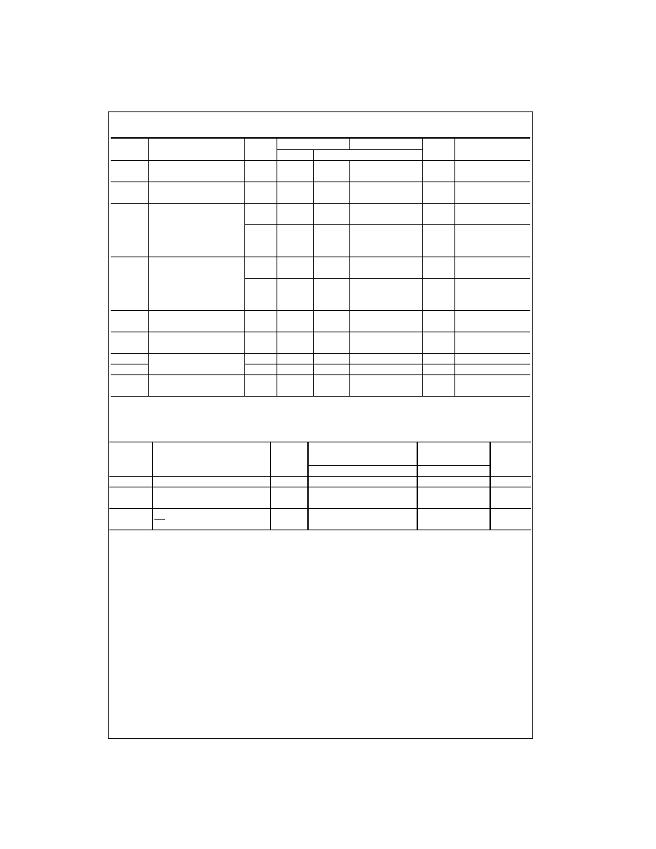
DC Electrical Characteristics for AC
Note 2: All outputs loaded; thresholds on input associated with output under test.
Note 3: Maximum test duration 2.0 ms, one output loaded at a time.
Note 4: I
IN
and I
CC
@ 3.0V are guaranteed to be less than or equal to the respective limit @ 5.5V V
CC
.
Supply Voltage (V
CC
)
-
0.5V to
+
7.0V
DC Input Diode Current (I
IK
)
V
I
=
-
0.5V
-
20 mA
V
I
=
V
CC
+
0.5V
+
20 mA
DC Input Voltage (V
I
)
-
0.5V to V
CC
+
0.5V
DC Output Diode Current (I
OK
)
V
O
=
-
0.5V
-
20 mA
V
O
=
V
CC
+
0.5V
+
20 mA
DC Output Voltage (V
O
)
-
0.5V to V
CC
+
0.5V
DC Output Source
or Sink Current (I
O
)
±
50 mA
DC V
CC
or Ground Current
per Output Pin (I
CC
or I
GND
)
±
50 mA
Storage Temperature (T
STG
)
-
65
∞
C to
+
150
∞
C
Junction Temperature (T
J
)
(PDIP)
140
∞
C
Supply Voltage (V
CC
)
AC
2.0V to 6.0V
ACT
4.5V to 5.5V
Input Voltage (V
I
)
0V to V
CC
Output Voltage (V
O
)
0V to V
CC
Operating Temperature (T
A
)
-
40
∞
C to
+
85
∞
C
Minimum Input Edge Rate (
V/
t)
AC Devices
V
IN
from 30% to 70% of V
CC
V
CC
@ 3.3V, 4.5V, 5.5V for AC
125 mV/ns
Minimum Input Edge Rate (
V/
t)
ACT Devices
V
IN
from 0.8V to 2.0V
V
CC
@ 4.5V, 5.5V for ACT
125 mV/ns
Symbol
Parameter
V
CC
T
A
=
+
25
∞
C
T
A
=
-
40
∞
C to
+
85
∞
C
Units
Conditions
(V)
Typ
Guaranteed Limits
V
IH
Minimum HIGH Level
3.0
1.5
2.1
2.1
V
OUT
=
0.1V
Input Voltage
4.5
2.25
3.15
3.15
V
or V
CC
-
0.1V
5.5
2.75
3.85
3.85
V
IL
Maximum LOW Level
3.0
1.5
0.9
0.9
V
OUT
=
0.1V
Input Voltage
4.5
2.25
1.35
1.35
V
or V
CC
-
0.1V
5.5
2.75
1.65
1.65
V
OH
Minimum HIGH Level
3.0
2.99
2.9
2.9
Output Voltage
4.5
4.49
4.4
4.4
V
I
OUT
=
-
50
µ
A
5.5
5.49
5.4
5.4
V
IN
=
V
IL
or V
IH
3.0
2.56
2.46
I
OH
=
-
12 mA
4.5
3.86
3.76
V
I
OH
=
-
24 mA
5.5
4.86
4.76
I
OH
=
-
24 mA (Note 2)
V
OL
Maximum LOW Level
3.0
0.002
0.1
0.1
Output Voltage
4.5
0.001
0.1
0.1
V
I
OUT
=
50
µ
A
5.5
0.001
0.1
0.1
V
IN
=
V
IL
or V
IH
3.0
0.36
0.44
I
OL
=
12 mA
4.5
0.36
0.44
V
I
OL
=
24 mA
5.5
0.36
0.44
I
OL
=
24 mA (Note 2)
I
IN
Maximum Input
5.5
±
0.1
±
1.0
µ
A
V
I
=
V
CC
, GND
(Note 4)
Leakage Current
I
OLD
Minimum Dynamic
5.5
75
mA
V
OLD
=
1.65V Max
I
OHD
Output Current (Note 3)
5.5
-
75
mA
V
OHD
=
3.85V Min
I
CC
Maximum Quiescent
5.5
4.0
40.0
µ
A
V
IN
=
V
CC
(Note 4)
Supply Current
or GND
www.fairchildsemi.com
4
74AC273
∑
74ACT273
AC Electrical Characteristics for AC
Note 5: Voltage Range 3.3 is 3.3V
±
0.3V
Voltage Range 5.0 is 5.0V
±
0.5V
AC Operating Requirements for AC
Note 6: Voltage Range 3.3 is 3.3V
±
0.3V
Voltage Range 5.0 is 5.0V
±
0.5V
V
CC
T
A
=
+
25
∞
C
T
A
=
-
40
∞
C to
+
85
∞
C
Symbol
Parameter
(V)
C
L
=
50 pF
C
L
=
50 pF
Units
(Note 5)
Min
Typ
Max
Min
Max
f
MAX
Maximum Clock
3.3
90
125
75
MHz
Frequency
5.0
140
175
125
t
PLH
Propagation Delay
3.3
4.0
7.0
12.5
3.0
14.0
ns
Clock to Output
5.0
3.0
5.5
9.0
2.5
10.0
t
PHL
Propagation Delay
3.3
4.0
7.0
13.0
3.5
14.5
ns
Clock to Output
5.0
3.0
5.0
10.0
2.5
11.0
t
PHL
Propagation Delay
3.3
4.0
7.0
13.0
3.5
14.0
ns
MR to Output
5.0
3.0
5.0
10.0
2.5
10.5
V
CC
T
A
=
+
25
∞
C
T
A
=
-
40
∞
C to
+
85
∞
C
Symbol
Parameter
(V)
C
L
=
50 pF
C
L
=
50 pF
Units
(Note 6)
Typ
Guaranteed Minimum
t
S
Setup Time, HIGH or LOW
3.3
3.5
5.5
6.0
ns
Data to CP
5.0
2.5
4.0
4.5
t
H
Hold Time, HIGH or LOW
3.3
-
2.0
0
0
ns
Data to CP
5.0
-
1.0
1.0
1.0
t
W
Clock Pulse Width
3.3
3.5
5.5
6.0
ns
HIGH or LOW
5.0
2.5
4.0
4.5
t
W
MR Pulse Width
3.3
2.0
5.5
6.0
ns
HIGH or LOW
5.0
1.5
4.0
4.5
t
rec
Recovery Time
3.3
1.5
3.5
4.5
ns
MR to CP
5.0
1.0
2.0
3.0
5
www.fairchildsemi.com
74
A
C
27
3
∑
74ACT273
DC Electrical Characteristics for ACT
Note 7: All outputs loaded; thresholds on input associated with output under test.
Note 8: Maximum test duration 2.0 ms, one output loaded at a time.
AC Electrical Characteristics for ACT
Note 9: Voltage Range 5.0 is 5.0V
±
0.5V
Symbol
Parameter
V
CC
T
A
=
+
25
∞
C
T
A
=
-
40
∞
C to
+
85
∞
C
Units
Conditions
(V)
Typ
Guaranteed Limits
V
IH
Minimum HIGH Level
4.5
1.5
2.0
2.0
V
V
OUT
=
0.1V
Input Voltage
5.5
1.5
2.0
2.0
or V
CC
-
0.1V
V
IL
Maximum LOW Level
4.5
1.5
0.8
0.8
V
V
OUT
=
0.1V
Input Voltage
5.5
1.5
0.8
0.8
or V
CC
-
0.1V
V
OH
Minimum HIGH Level
4.5
4.49
4.4
4.4
V
I
OUT
=
-
50
µ
A
Output Voltage
5.5
5.49
5.4
5.4
V
IN
=
V
IL
or V
IH
4.5
3.86
3.76
V
I
OH
=
-
24 mA
5.5
4.86
4.76
I
OH
=
-
24 mA (Note 7)
V
OL
Maximum LOW Level
4.5
0.001
0.1
0.1
V
I
OUT
=
50
µ
A
Output Voltage
5.5
0.001
0.1
0.1
V
IN
=
V
IL
or V
IH
4.5
0.36
0.44
V
I
OL
=
24 mA
5.5
0.36
0.44
I
OL
=
24 mA (Note 7)
I
IN
Maximum Input
5.5
±
0.1
±
1.0
µ
A
V
I
=
V
CC
, GND
Leakage Current
I
CCT
Maximum
5.5
0.6
1.5
mA
V
I
=
V
CC
-
2.1V
I
CC
/Input
I
OLD
Minimum Dynamic
5.5
75
mA
V
OLD
=
1.65V Max
I
OHD
Output Current (Note 8)
5.5
-
75
mA
V
OHD
=
3.85V Min
I
CC
Maximum Quiescent
5.5
4.0
40.0
µ
A
V
IN
=
V
CC
Supply Current
or GND
V
CC
T
A
=
+
25
∞
C
T
A
=
-
40
∞
C to
+
85
∞
C
Symbol
Parameter
(V)
C
L
=
50 pF
C
L
=
50 pF
Units
(Note 9)
Min
Typ
Max
Min
Max
f
MAX
Maximum Clock Frequency
2.0
125
189
110
MHz
t
PLH
Propagation Delay
5.0
1.5
6.5
8.5
1.5
9.0
ns
t
PHL
CP to Q
n
t
PHL
Propagation Delay
5.0
1.5
7.0
9.0
1.5
8.5
ns
MR to Q
n