74LVQ14
Low Voltage Hex Inverter with Schmitt Trigger Input
General Description
The LVQ14 contains six inverter gates each with a Schmitt
trigger input. They are capable of transforming slowly chang-
ing input signals into sharply defined, jitter-free output sig-
nals. In addition, they have a greater noise margin than con-
ventional inverters.
The LVQ14 has hysteresis between the positive-going and
negative-going input thresholds (typically 1.0V) which is de-
termined internally by transistor ratios and is essentially in-
sensitive to temperature and supply voltage variations.
Features
n
Ideal for low power/low noise 3.3V applications
n
Guaranteed simultaneous switching noise level and
dynamic threshold performance
n
Guaranteed pin-to-pin skew AC performance
n
Guaranteed incident wave switching into 75
Ordering Code:
Order Number
Package Number
Package Description
74LVQ14SC
M14A
14-Lead (0.150" Wide) Molded Small Outline Integrated Circuit, SOIC JEDEC
74LVQ14SJ
M14D
14-Lead Small Outline Package, SOIC EIAJ
Devices also available in Tape and Reel. Specify by appending the suffix letter "X" to the ordering code.
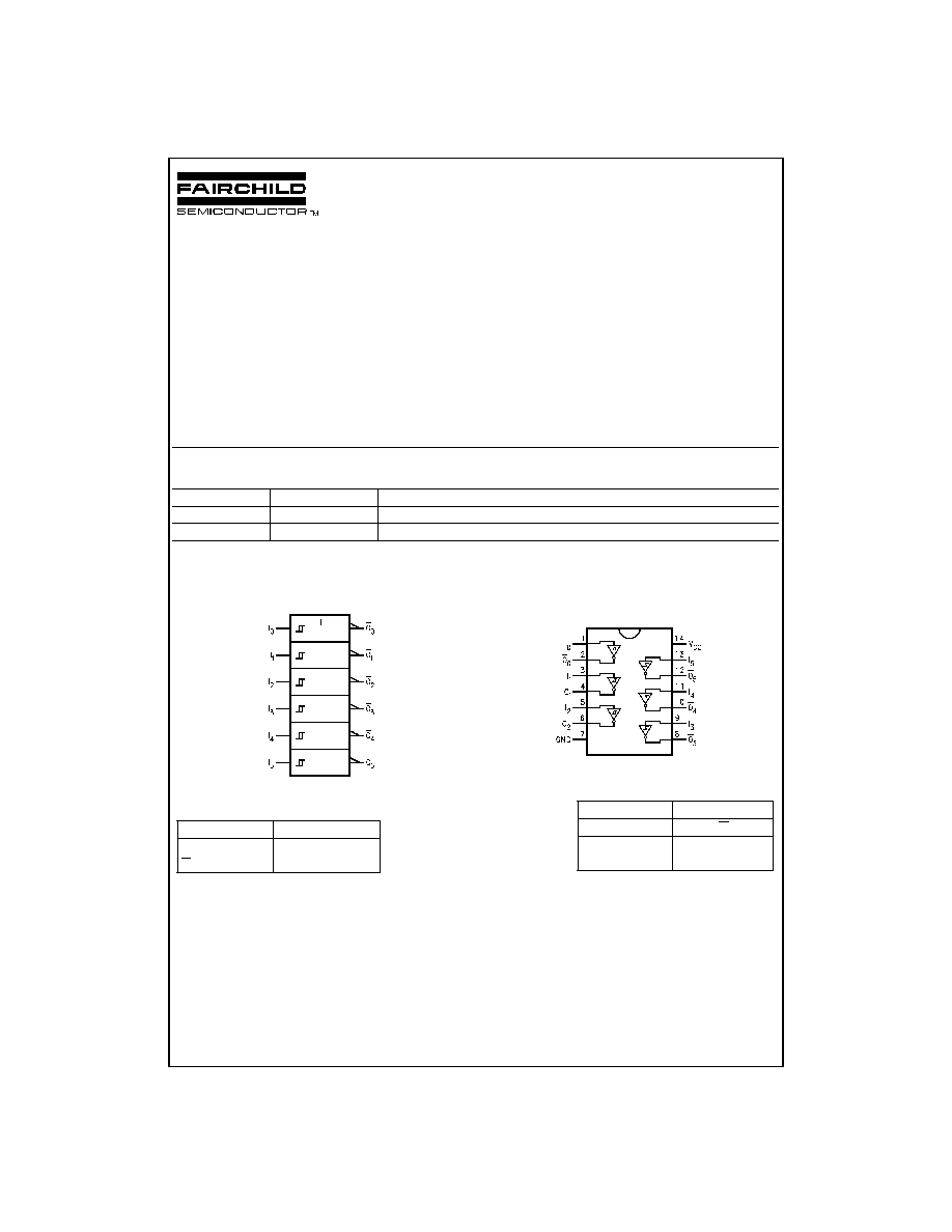
Logic Symbol
Pin Descriptions
Pin Names
Description
I
n
Inputs
O
n
Outputs
Connection Diagram
Truth Table
Input
Output
I
O
L
H
H
L
H = High Voltage Level
L = Low Voltage Level
IEEE/IEC
DS011345-1
Pin Assignment
for SOIC JEDEC and EIAJ
DS011345-2
May 1998
74L
VQ14
Low
V
oltage
Hex
Inverter
with
Schmitt
T
rigger
Input
� 1998 Fairchild Semiconductor Corporation
DS011345
www.fairchildsemi.com

Absolute Maximum Ratings
(Note 1)
Supply Voltage (V
CC
)
-0.5V to +7.0V
DC Input Diode Current (I
IK
)
V
I
= -0.5V
-20 mA
V
I
= V
CC
+ 0.5V
+20 mA
DC Input Voltage (V
I
)
-0.5V to V
CC
+ 0.5V
DC Output Diode Current (I
OK
)
V
O
= -0.5V
-20 mA
V
O
= V
CC
+ 0.5V
+20 mA
DC Output Voltage (V
O
)
-0.5V to to V
CC
+ 0.5V
DC Output Source
or Sink Current (I
O
)
�
50 mA
DC V
CC
or Ground Current
(I
CC
or I
GND
)
�
200 mA
Storage Temperature (T
STG
)
-65�C to +150�C
DC Latch-Up Source or
Sink Current
�
100 mA
Recommended Operating
Conditions
(Note 2)
Supply Voltage (V
CC
)
LVQ
2.0V to 3.6V
Input Voltage (V
I
)
0V to V
CC
Output Voltage (V
O
)
0V to V
CC
Operating Temperature (T
A
)
-40�C to +85�C
Minimum Input Edge Rate (
V/
t)
V
IN
from 0.8V to 2.0V
V
CC
@
3.0V
125 mV/ns
Note 1: The "Absolute Maximum Ratings" are those values beyond which
the safety of the device cannot be guaranteed. The device should not be op-
erated at these limits. The parametric values defined in the Electrical Charac-
teristics tables are not guaranteed at the absolute maximum ratings. The
"Recommended Operating Conditions" table will define the conditions for ac-
tual device operation.
Note 2: Unused inputs must be held HIGH or LOW. They may not float.
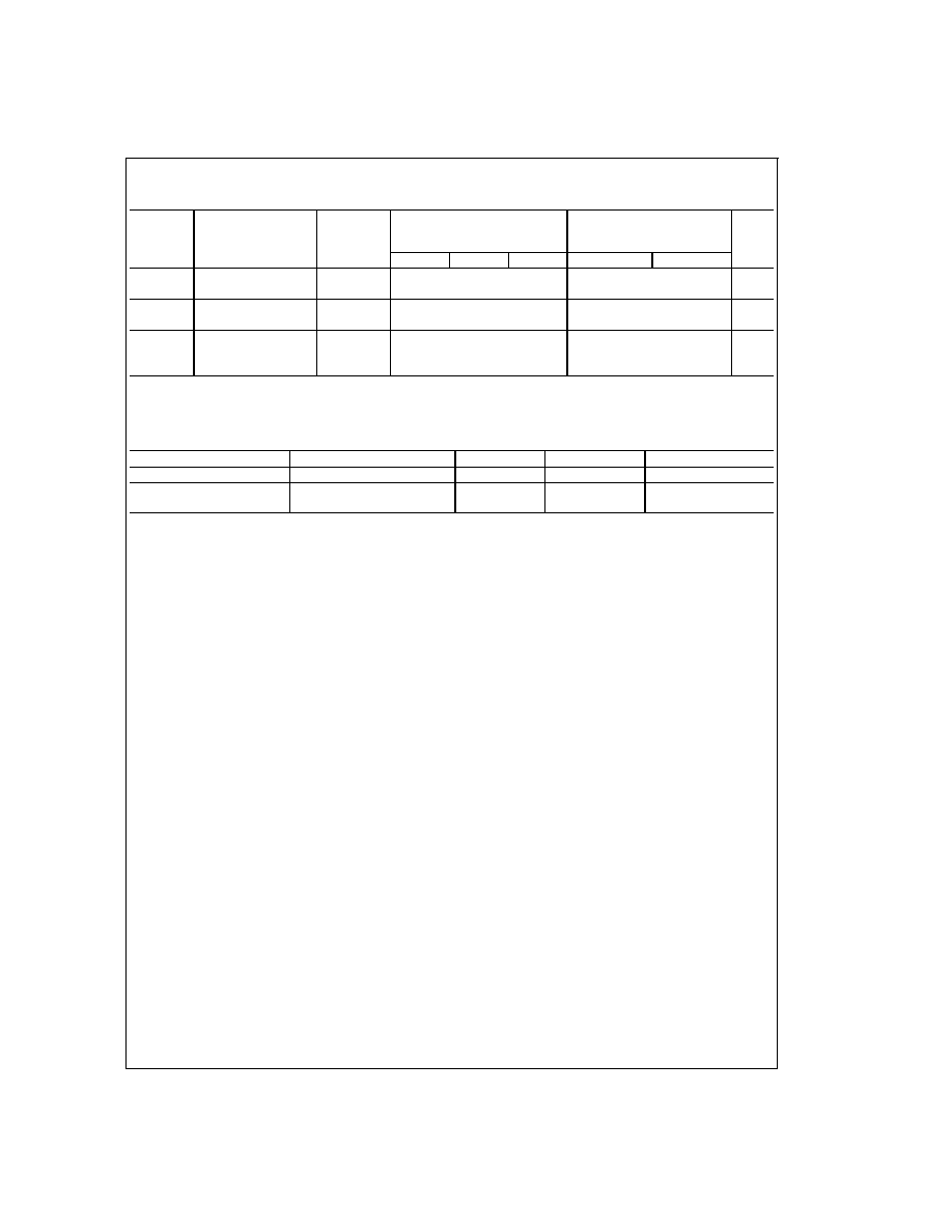
DC Electrical Characteristics
Symbol
Parameter
V
CC
(V)
T
A
= +25�C
T
A
= -40�C to +85�C
Units
Conditions
Typ
Guaranteed Limits
V
OH
Minimum High Level
Output Voltage
3.0
2.99
2.9
2.9
V
I
OUT
= -50 �A
3.0
2.58
2.48
V
V
IN
= V
IL
or V
IH
(Note 3)
I
OH
= -12 mA
V
OL
Maximum Low Level
Output Voltage
3.0
0.002
0.1
0.1
V
I
OUT
= 50 �A
3.0
0.36
0.44
V
V
IN
= V
IL
or V
IH
(Note 3)
I
OL
= 12 mA
I
IN
Maximum Input
Leakage Current
3.6
�
0.1
�
1.0
�A
V
I
= V
CC
, GND
V
t+
Maximum Positive
Threshold
3.0
2.2
2.2
V
T
A
= Worst Case
V
t-
Minimum Negative
Threshold
3.0
0.5
0.5
V
T
A
= Worst Case
V
h(max)
Maximum Hysteresis
3.0
1.2
1.2
V
T
A
= Worst Case
V
h(min)
Minimum Hysteresis
3.0
0.3
0.3
V
T
A
= Worst Case
I
OLD
Minimum Dynamic (Note 4)
Output Current
3.6
36
mA
V
OLD
= 0.8V Max (Note 5)
I
OHD
3.6
-25
mA
V
OHD
= 2.0V Min (Note 5)
I
CC
Maximum Quiescent
Supply Current
3.6
2.0
20.0
�A
V
IN
= V
CC
or GND
V
OLP
Quiet Output
Maximum Dynamic V
OL
3.3
0.9
1.1
V
(Notes 6, 7)
V
OLV
Quiet Output
Minimum Dynamic V
OL
3.3
-0.8
-1.1
V
(Notes 6, 7)
V
IHD
Maximum High Level
Dynamic Input Voltage
3.3
1.9
2.0
V
(Notes 6, 8)
V
ILD
Maximum Low Level
Dynamic Input Voltage
3.3
1.3
2.0
V
(Notes 6, 8)
Note 3: All outputs loaded; thresholds on input associated with output under test.
Note 4: Maximum test duration 2.0 ms, one output loaded at a time.
Note 5: Incident wave switching on transmission lines with impedances as low as 75
for commercial temperature range is guaranteed for 74LVQ.
Note 6: Worst case package.
Note 7: Max number of outputs defined as (n). Data inputs are driven 0V to 3.3V; one output at GND.
Note 8: Max number of Data Inputs (n) switching. (n - 1) inputs switching 0V to 3.3V. Input-under-test switching: 3.3V to threshold (V
ILD
), 0V to threshold (V
IHD
),
f = 1 MHz.
www.fairchildsemi.com
2
AC Electrical Characteristics
Symbol
Parameter
V
CC
(V)
Units
T
A
= +25�C
C
L
= 50 pF
T
A
= -40�C to +85�C
C
L
= 50 pF
Min
Typ
Max
Min
Max
t
PLH
Propagation Delay
2.7
1.5
11.4
19.0
1.5
21.0
ns
3.3
�
0.3
1.5
9.5
13.5
1.5
15.0
t
PHL
Propagation Delay
2.7
1.5
9.0
16.2
1.5
19.0
ns
3.3
�
0.3
1.5
7.5
11.5
1.5
13.0
t
OSHL,
Output to Output
2.7
1.0
1.5
1.5
ns
t
OSLH
Skew (Note 9)
3.3
�
0.3
1.0
1.5
1.5
Data to Output
Note 9: Skew is defined as the absolute value of the difference between the actual propagation delay for any two separate outputs of the same device. The speci-
fication applies to any outputs switching in the same direction, either HIGH to LOW (t
OSHL
) or LOW to HIGH (t
OSLH
). Parameter guaranteed by design.
Capacitance
Symbol
Parameter
Typ
Units
Conditions
C
IN
Input Capacitance
4.5
pF
V
CC
= Open
C
PD
(Note 10)
Power Dissipation
20
pF
V
CC
= 3.3V
Capacitance
Note 10: C
PD
is measured at 10 MHz.
3
www.fairchildsemi.com

