© 2005 Fairchild Semiconductor Corporation
DS012446
www.fairchildsemi.com
January 1999
Revised June 2005
7
4
L
V
T1
62245
· 74L
VTH162245 Low
V
o
lt
age 16-Bi
t T
r
ans
ceiver
wi
th
3
-
ST
A
T
E
Output
s and
25
:
Seri
es Resi
stor
s i
n
A Port
Out
put
s
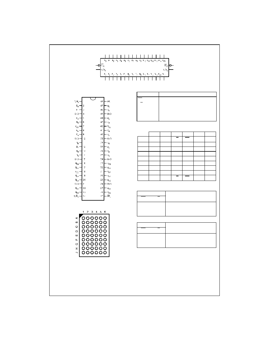
74LVT162245 · 74LVTH162245
Low Voltage 16-Bit Transceiver with 3-STATE Outputs
and 25
:
Series Resistors in A Port Outputs
General Description
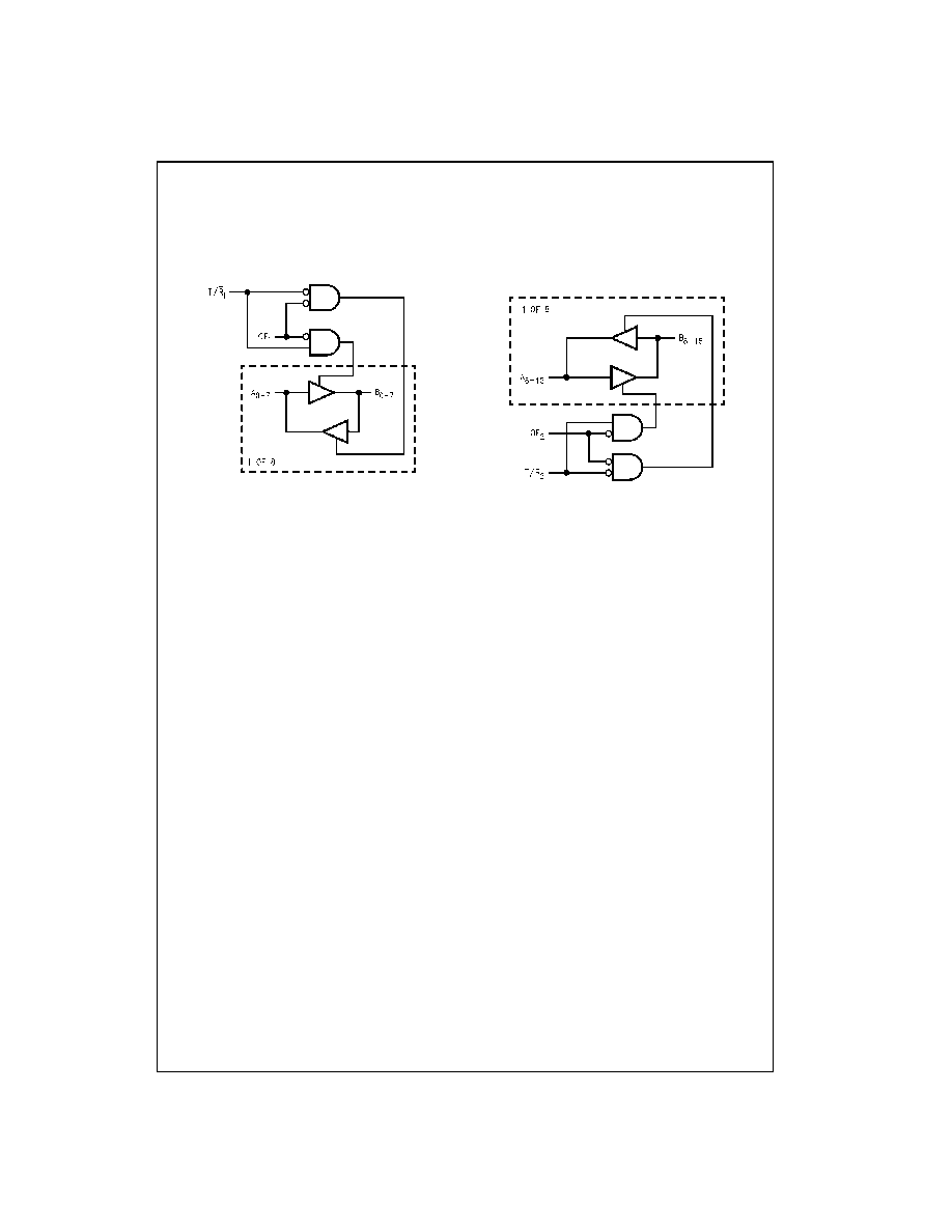
The LVT162245 and LVTH162245 contains sixteen non-
inverting bidirectional buffers with 3-STATE outputs and is
intended for bus oriented applications. The device is byte
controlled. Each byte has separate control inputs which
can be shorted together for full 16-bit operation. The T/R
inputs determine the direction of data flow through the
device. The OE inputs disable both the A and B ports by
placing them in a high impedance state.
The LVT162245 and LVTH162245 are designed with
equivalent 25
:
series resistance in both the HIGH and
LOW states on the A Port outputs. This design reduces line
noise in applications such as memory address drivers,
clock drivers, and bus transceivers/transmitters.
The LVTH162245 data inputs include bushold, eliminating
the need for external pull-up resistors to hold unused
inputs.
These non-inverting transceivers are designed for low volt-
age (3.3V) V
CC
applications, but with the capability to pro-
vide a TTL interface to a 5V environment. The LVT162245
and LVTH162245 are fabricated with an advanced
BiCMOS technology to achieve high speed operation simi-
lar to 5V ABT while maintaining a low power dissipation.
Features
s
Input and output interface capability to systems at
5V V
CC
s
Bushold data inputs eliminate the need for external pull-
up resistors to hold unused inputs (74LVTH162245),
also available without bushold feature (74LVT162245).
s
Live insertion/extraction permitted
s
Power Up/Down high impedance provides glitch-free
bus loading
s
A Port outputs include equivalent series resistance of
25
:
making external termination resistors unnecessary
and reducing overshoot and undershoot
s
A Port outputs source/sink
r
12 mA.
B Port outputs source/sink
32 mA/
64 mA
s
Functionally compatible with the 74 series 162245
s
Latch-up performance exceeds 500 mA
s
ESD performance:
Human-body model
!
2000V
Machine model
!
200V
Charged-device model
!
1000V
s
Also packaged in plastic Fine Pitch Ball Grid Array
(FBGA)
Ordering Code:
Note 1: Ordering code "G" indicates Trays.
Note 2: Devices also available in Tape and Reel. Specify by appending the suffix letter "X" to the ordering code.
Order Number
Package Number
Package Description
74LVT162245G
(Note 1)(Note 2)
BGA54A
(Preliminary)
54-Ball Fine-Pitch Ball Grid Array (FBGA), JEDEC MO-205, 5.5mm Wide
74LVT162245MEA
(Note 2)
MS48A
48-Lead Small Shrink Outline Package (SSOP), JEDEC MO-118, 0.300" Wide
74LVT162245MTD
(Note 2)
MTD48
48-Lead Thin Shrink Small Outline Package (TSSOP), JEDEC MO-153, 6.1mm Wide
74LVTH162245G
(Note 1)(Note 2)
BGA54A
54-Ball Fine-Pitch Ball Grid Array (FBGA), JEDEC MO-205, 5.5mm Wide
74LVTH162245MEA
MS48A
48-Lead Small Shrink Outline Package (SSOP), JEDEC MO-118, 0.300" Wide
[TUBE]
74LVTH162245MEX
MS48A
48-Lead Small Shrink Outline Package (SSOP), JEDEC MO-118, 0.300" Wide
[TAPE and REEL]
74LVTH162245MTD
MTD48
48-Lead Thin Shrink Small Outline Package (TSSOP), JEDEC MO-153, 6.1mm Wide
[TUBE]
74LVTH162245MTX
MTD48
48-Lead Thin Shrink Small Outline Package (TSSOP), JEDEC MO-153, 6.1mm Wide
[TAPE and REEL]
www.fairchildsemi.com
4
7
4
L
V
T1
62245
·
74L
VTH162245
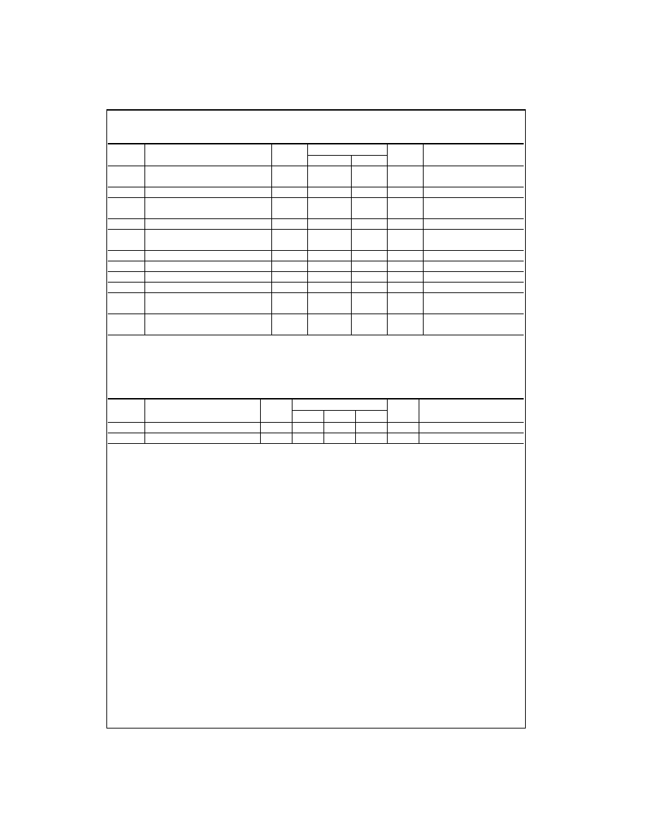
Absolute Maximum Ratings
(Note 3)
Recommended Operating Conditions
Note 3: Absolute Maximum continuous ratings are those values beyond which damage to the device may occur. Exposure to these conditions or conditions
beyond those indicated may adversely affect device reliability. Functional operation under absolute maximum rated conditions is not implied.
Note 4: I
O
Absolute Maximum Rating must be observed.
DC Electrical Characteristics
Symbol
Parameter
Value
Conditions
Units
V
CC
Supply Voltage
0.5 to
4.6
V
V
I
DC Input Voltage
0.5 to
7.0
V
V
O
Output Voltage
0.5 to
7.0
Output in 3-STATE
V
0.5 to
7.0
Output in HIGH or LOW State (Note 4)
I
IK
DC Input Diode Current
50
V
I
GND
mA
I
OK
DC Output Diode Current
50
V
O
GND
mA
I
O
DC Output Current
64
V
O
!
V
CC
Output at HIGH State
mA
128
V
O
!
V
CC
Output at LOW State
I
CC
DC Supply Current per Supply Pin
r
64
mA
I
GND
DC Ground Current per Ground Pin
r
128
mA
T
STG
Storage Temperature
65 to
150
q
C
Symbol
Parameter
Min
Max
Units
V
CC
Supply Voltage
2.7
3.6
V
V
I
Input Voltage
0
5.5
V
I
OH
HIGH-Level Output Current
B Port
32
mA
A Port
12
I
OL
LOW-Level Output Current
B Port
64
mA
A Port
12
T
A
Free Air Operating Temperature
40
85
q
C
'
t/
'
V
Input Edge Rate, V
IN
0.8V2.0V, V
CC
3.0V
0
10
ns/V
Symbol
Parameter
V
CC
T
A
40
q
C to
85
q
C
Units
Conditions
(V)
Min
Max
V
IK
Input Clamp Diode Voltage
2.7
1.2
V
I
I
18 mA
V
IH
Input HIGH Voltage
2.73.6
2.0
V
V
O
d
0.1V or
V
IL
Input LOW Voltage
2.73.6
0.8
V
V
O
t
V
CC
0.1V
V
OH
Output HIGH Voltage
A Port
3.0
2.0
V
I
OH
12 mA
2.73.6
V
CC
0.2
V
I
OH
100
P
A
B Port
2.7
2.4
V
I
OH
8 mA
3.0
2.0
I
OH
32 mA
V
OL
Output LOW Voltage
A Port
3.0
0.8
V
I
OL
12 mA
2.7
0.2
V
I
OL
100
P
A
B Port
2.7
0.5
V
I
OL
24 mA
3.0
0.4
I
OL
16 mA
3.0
0.5
I
OL
32 mA
3.0
0.55
I
OL
64 mA
I
I(HOLD)
Bushold Input Minimum Drive
3.0
75
P
A
V
I
0.8V
(Note 5)
75
V
I
2.0V
I
I(OD)
Bushold Input Over-Drive
3.0
500
P
A
(Note 6)
(Note 5)
Current to Change State
500
(Note 7)
I
I
Input Current
3.6
10
P
A
V
I
5.5V
Control Pins
3.6
r
1
V
I
0V or V
CC
Data Pins
3.6
5
V
I
0V
1
V
I
V
CC
I
OFF
Power Off Leakage Current
0
r
100
P
A
0V
d
V
I
or V
O
d
5.5V
5
www.fairchildsemi.com
7
4
L
V
T1
62245
·
74L
VTH162245
DC Electrical Characteristics
(Continued)
Note 5: Applies to Bushold versions only (74LVTH162245).
Note 6: An external driver must source at least the specified current to switch from LOW-to-HIGH.
Note 7: An external driver must sink at least the specified current to switch from HIGH-to-LOW.
Note 8: This is the increase in supply current for each input that is at the specified voltage level rather than V
CC
or GND.
Dynamic Switching Characteristics
(Note 9)
Note 9: Characterized in SSOP package. Guaranteed parameter, but not tested.
Note 10: Max number of outputs defined as (n). n
1 data inputs are driven 0V to 3V. Output under test held LOW.
Symbol
Parameter
V
CC
T
A
40
q
C to
85
q
C
Units
Conditions
(V)
Min
Max
I
PU/PD
Power Up/Down
01.5V
r
100
P
A
V
O
0.5V to 3.0V
3-STATE Current
V
I
GND to V
CC
I
OZL
3-STATE Output Leakage Current
3.6
5
P
A
V
O
0.5V
I
OZL
3-STATE Output Leakage Current
3.6
5
P
A
V
O
0.0V
(Note 5)
I
OZH
3-STATE Output Leakage Current
3.6
5
P
A
V
O
3.0V
I
OZH
3-STATE Output Leakage Current
3.6
5
P
A
V
O
3.6V
(Note 5)
I
OZH
3-STATE Output Leakage Current
3.6
10
P
A
V
CC
V
O
d
5.5V
I
CCH
Power Supply Current
3.6
0.19
mA
Outputs HIGH
I
CCL
Power Supply Current
3.6
5
mA
Outputs LOW
I
CCZ
Power Supply Current
3.6
0.19
mA
Outputs Disabled
I
CCZ
Power Supply Current
3.6
0.19
mA
V
CC
d
V
O
d
5.5V,
Outputs Disabled
'
I
CC
Increase in Power Supply Current
3.6
0.2
mA
One Input at V
CC
0.6V
(Note 8)
Other Inputs at V
CC
or GND
Symbol
Parameter
V
CC
T
A
25
q
C
Units
Conditions
(V)
Min
Typ
Max
C
L
50 pF, R
L
500
:
V
OLP
Quiet Output Maximum Dynamic V
OL
3.3
0.8
V
(Note 10)
V
OLV
Quiet Output Minimum Dynamic V
OL
3.3
0.8
V
(Note 10)