© 2005 Fairchild Semiconductor Corporation
DS011516
www.fairchildsemi.com
November 1992
Revised February 2005
7
4
VH
C04
Hex
Inve
rte
r
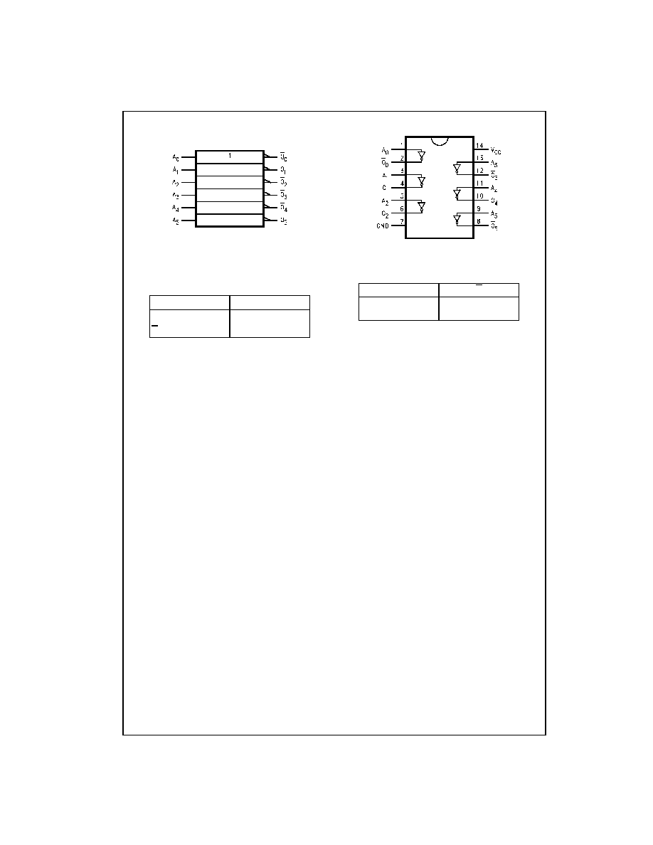
74VHC04
Hex Inverter
General Description
The VHC04 is an advanced high speed CMOS Inverter
fabricated with silicon gate CMOS technology. It achieves
the high speed operation similar to equivalent Bipolar
Schottky TTL while maintaining the CMOS low power dissi-
pation.
The internal circuit is composed of 3 stages including buffer
output, which provide high noise immunity and stable out-
put. An input protection circuit ensures that 0V to 7V can be
applied to the input pins without regard to the supply volt-
age. This device can be used to interface 5V to 3V systems
and two supply systems such as battery back up. This cir-
cuit prevents device destruction due to mismatched supply
and input voltages.
Features
s
High Speed: t
PD
3.8 ns (typ) at V
CC
5V
s
High noise immunity: V
NIH
V
NIL
28% V
CC
(Min)
s
Power down protection is provided on all inputs
s
Low Noise: V
OLP
0.4V (typ)
s
Low power dissipation: I
CC
2
P
A (Max) @ T
A
25
q
C
s
Pin and function compatible with 74HC04
Ordering Code:
Surface mount packages are also available on Tape and Reel. Specify by appending the suffix letter "X" to the ordering code.
Pb-Free package per JEDEC J-STD-020B.
Note 1: "_NL" indicates Pb-Free package (per JEDEC J-STD-020B). Device available in Tape and Reel only.
Order Number
Package
Package Description
Number
74VHC04M
M14A
14-Lead Small Outline Integrated Circuit (SOIC), JEDEC MS-012, 0.150" Narrow
74VHC04MX_NL
(Note 1)
M14A
Pb-Free 14-Lead Small Outline Integrated Circuit (SOIC), JEDEC MS-012, 0.150" Narrow
74VHC04SJ
M14D
Pb-Free 14-Lead Small Outline Package (SOP), EIAJ TYPE II, 5.3mm Wide
74VHC04MTC
MTC14
14-Lead Thin Shrink Small Outline Package (TSSOP), JEDEC MO-153, 4.4mm Wide
74VHC04MTCX_NL
(Note 1)
MTC14
Pb-Free 14-Lead Thin Shrink Small Outline Package (TSSOP), JEDEC MO-153, 4.4mm
Wide
74VHC04N
N14A
14-Lead Plastic Dual-In-Line Package (PDIP), JEDEC MS-001, 0.300" Wide
3
www.fairchildsemi.com
7
4
VH
C04
Absolute Maximum Ratings
(Note 2)
Recommended Operating
Conditions
(Note 3)
Note 2: Absolute Maximum Ratings are values beyond which the device
may be damaged or have its useful life impaired. The databook specifica-
tions should be met, without exception, to ensure that the system design is
reliable over its power supply, temperature, and output/input loading vari-
ables. Fairchild does not recommend operation outside databook specifica-
tions.
Note 3: Unused inputs must be held HIGH or LOW. They may not float.
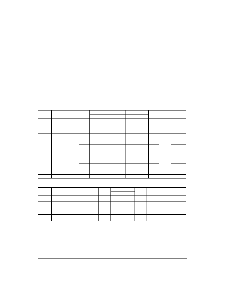
DC Electrical Characteristics
Noise Characteristics
Note 4: Parameter guaranteed by design.
Supply Voltage (V
CC
)
0.5V to
7.0V
DC Input Voltage (V
IN
)
0.5V to
7.0V
DC Output Voltage (V
OUT
)
0.5V to V
CC
0.5V
Input Diode Current (I
IK
)
20 mA
Output Diode Current (I
OK
)
r
20 mA
DC Output Current (I
OUT
)
r
25 mA
DC V
CC
/GND Current (I
CC
)
r
50 mA
Storage Temperature (T
STG
)
65
q
C to
150
q
C
Lead Temperature (T
L
)
(Soldering, 10 seconds)
260
q
C
Supply Voltage (V
CC
)
2.0V to
5.5V
Input Voltage (V
IN
)
0V to
5.5V
Output Voltage (V
OUT
)
0V to V
CC
Operating Temperature (T
OPR
)
40
q
C to
85
q
C
Input Rise and Fall Time (t
r
, t
f
)
V
CC
3.3V
r
0.3V
0
a
100 ns/V
V
CC
5.0V
r
0.5V
0
a
20 ns/V
Symbol
Parameter
V
CC
(V)
T
A
25
q
C
T
A
40
q
C to
85
q
C
Units
Conditions
Min
Typ
Max
Min
Max
V
IH
HIGH Level
2.0
1.50
1.50
V
Input Voltage
3.0
5.5
0.7 V
CC
0.7 V
CC
V
IL
LOW Level
2.0
0.50
0.50
V
Input Voltage
3.0
5.5
0.3 V
CC
0.3 V
CC
V
OH
HIGH Level
2.0
1.9
2.0
1.9
V
IN
V
IH
I
OH
50
P
A
Output Voltage
3.0
2.9
3.0
2.9
V
or V
IL
4.5
4.4
4.5
4.4
3.0
2.58
2.48
V
I
OH
4 mA
4.5
3.94
3.80
I
OH
8 mA
V
OL
LOW Level
2.0
0.0
0.1
0.1
V
IN
V
IH
I
OL
50
P
A
Output Voltage
3.0
0.0
0.1
0.1
V
or V
IL
4.5
0.0
0.1
0.1
3.0
0.36
0.44
V
I
OL
4 mA
4.5
0.36
0.44
I
OL
8 mA
I
IN
Input Leakage Current
0
5.5
r
0.1
r
1.0
P
A
V
IN
5.5V or GND
I
CC
Quiescent Supply Current
5.5
2.0
20.0
P
A
V
IN
V
CC
or GND
Symbol
Parameter
V
CC
(V)
T
A
25
q
C
Units
Conditions
Typ
Limits
V
OLP
(Note 4)
Quiet Output Maximum Dynamic V
OL
5.0
0.4
0.8
V
C
L
50 pF
V
OLV
(Note 4)
Quiet Output Minimum Dynamic V
OL
5.0
0.4
0.8
V
C
L
50 pF
V
IHD
(Note 4)
Minimum HIGH Level Dynamic Input Voltage
5.0
3.5
V
C
L
50 pF
V
ILD
(Note 4)
Maximum LOW Level Dynamic Input Voltage
5.0
1.5
V
C
L
50 pF
www.fairchildsemi.com
4
7
4
VH
C04
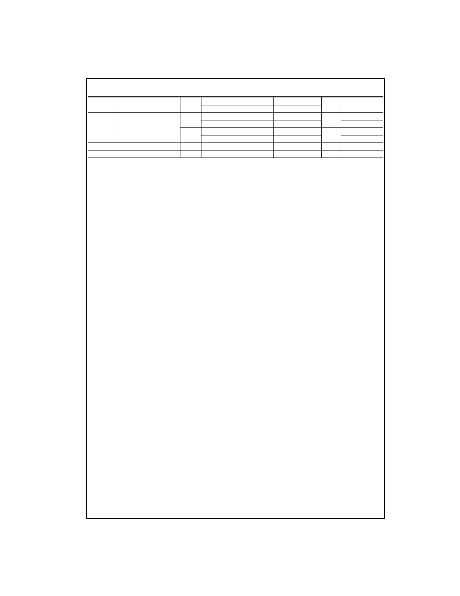
AC Electrical Characteristics
Note 5: C
PD
is defined as the value of the internal equivalent capacitance which is calculated from the operating current consumption without load. Average
operating current can be obtained by the equation: I
CC
(opr.)
C
PD
* V
CC
* f
IN
I
CC
/6 (per gate).
Symbol
Parameter
V
CC
(V)
T
A
25
q
C
T
A
40
q
C to
85
q
C
Units
Conditions
Min
Typ
Max
Min
Max
t
PHL
Propagation Delay
3.3
r
0.3
5.0
7.1
1.0
8.5
ns
C
L
15 pF
t
PLH
7.5
10.6
1.0
12.0
C
L
50 pF
5.0
r
0.5
3.8
5.5
1.0
6.5
ns
C
L
15 pF
5.3
7.5
1.0
8.5
C
L
50 pF
C
IN
Input Capacitance
4
10
10
pF
V
CC
OPEN
C
PD
Power Dissipation Capacitance
18
pF
(Note 5)
5
www.fairchildsemi.com
7
4
VH
C04
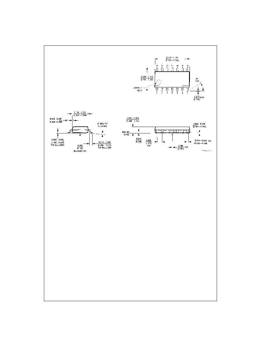
Physical Dimensions
inches (millimeters) unless otherwise noted
14-Lead Small Outline Integrated Circuit (SOIC), JEDEC MS-012, 0.150" Narrow
Package Number M14A