 | –≠–ª–µ–∫—Ç—Ä–æ–Ω–Ω—ã–π –∫–æ–º–ø–æ–Ω–µ–Ω—Ç: 74VHC132M | –°–∫–∞—á–∞—Ç—å:  PDF PDF  ZIP ZIP |

© 2005 Fairchild Semiconductor Corporation
DS012124
www.fairchildsemi.com
September 1995
Revised February 2005
7
4
VH
C13
2
Quad
2-I
nput
NAND Schmit
t
T
r
igger
74VHC132
Quad 2-Input NAND Schmitt Trigger
General Description
The VHC132 is an advanced high speed CMOS 2-input
NAND Schmitt Trigger Gate fabricated with silicon gate
CMOS technology. It achieves the high-speed operation
similar to Bipolar Schottky TTL while maintaining the
CMOS low power dissipation. Pin configuration and func-
tion are the same as the VHC00 but the inputs have hyster-
esis between the positive-going and negative-going input
thresholds, which are capable of transforming slowly
changing input signals into sharply defined, jitter-free out-
put signals. Thus greater noise margin then conventional
gates is provided. An input protection circuit ensures that
0V to 7V can be applied to the input pins without regard to
the supply voltage. This device can be used to interface 5V
to 3V systems and two supply systems such as battery
backup. This circuit prevents device destruction due to mis-
matched supply and input voltages.
Features
s
High Speed: t
PD
3.9 ns (typ) at V
CC
5 V
s
Power down protection is provided on all inputs
s
Low power dissipation: I
CC
2
P
A (max) at T
A
25
q
C
s
Low noise: V
OLP
0.8 V (max)
s
Pin and function compatible with 74HC132
Ordering Code:
Surface mount packages are also available on Tape and Reel. Specify by appending the suffix letter "X" to the ordering code.
Pb-Free package per JEDEC J-STD-020B.
Note 1: "_NL" indicates Pb-Free package (per JEDEC J-STD-020B). Device available in Tape and Reel only.
Order Number
Package
Package Description
Number
74VHC132M
M14A
14-Lead Small Outline Integrated Circuit (SOIC), JEDEC MS-012, 0.150" Narrow
74VHC132SJ
M14D
Pb-Free 14-Lead Small Outline Package (SOP), EIAJ TYPE II, 5.3mm Wide
74VHC132MTC
MTC14
14-Lead Thin Shrink Small Outline Package (TSSOP), JEDEC MO-153, 4.4mm Wide
74VHC132MTCX_NL
(Note 1)
MTC14
Pb-Free 14-Lead Thin Shrink Small Outline Package (TSSOP), JEDEC MO-153, 4.4mm
Wide
74VHC132N
N14A
14-Lead Plastic Dual-In-Line Package (PDIP), JEDEC MS-001, 0.300" Wide

www.fairchildsemi.com
2
74
V
HC132
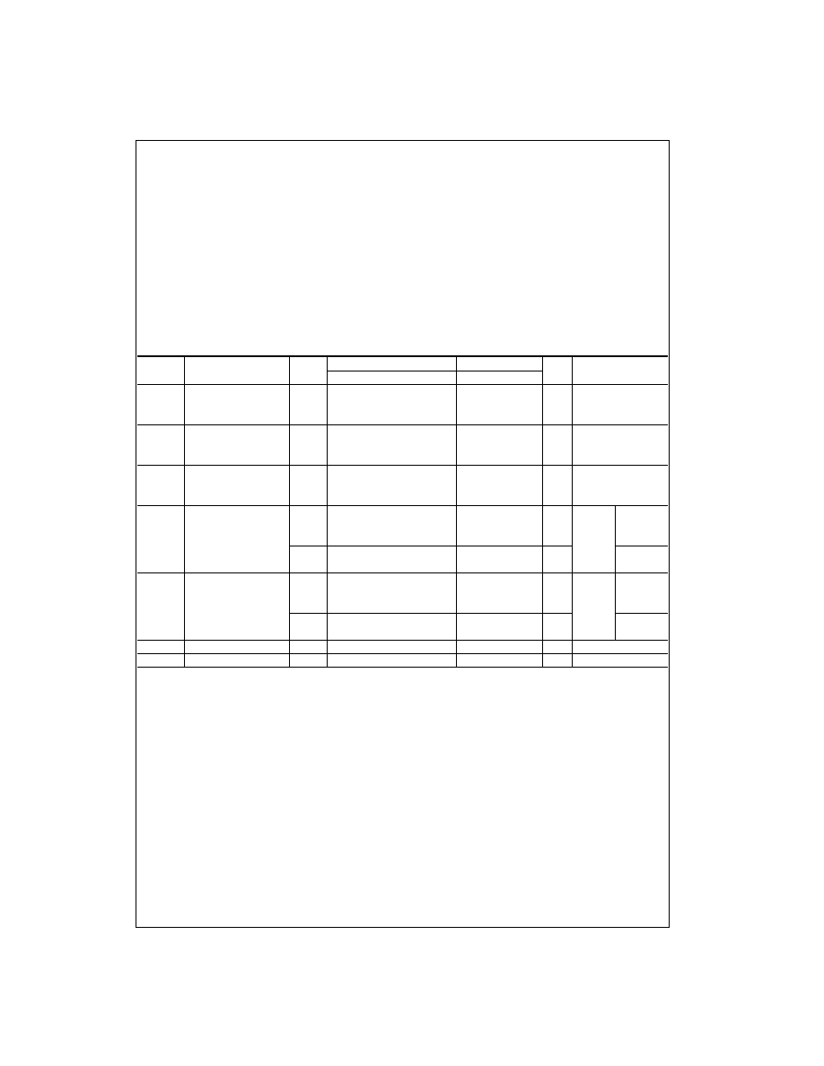
Connection Diagram
Pin Descriptions
Logic Diagram
Truth Table
Pin Names
Description
A
n
, B
n
Inputs
Y
n
Outputs
A
B
Y
L
L
H
L
H
H
H
L
H
H
H
L
3
www.fairchildsemi.com
7
4
VH
C13
2
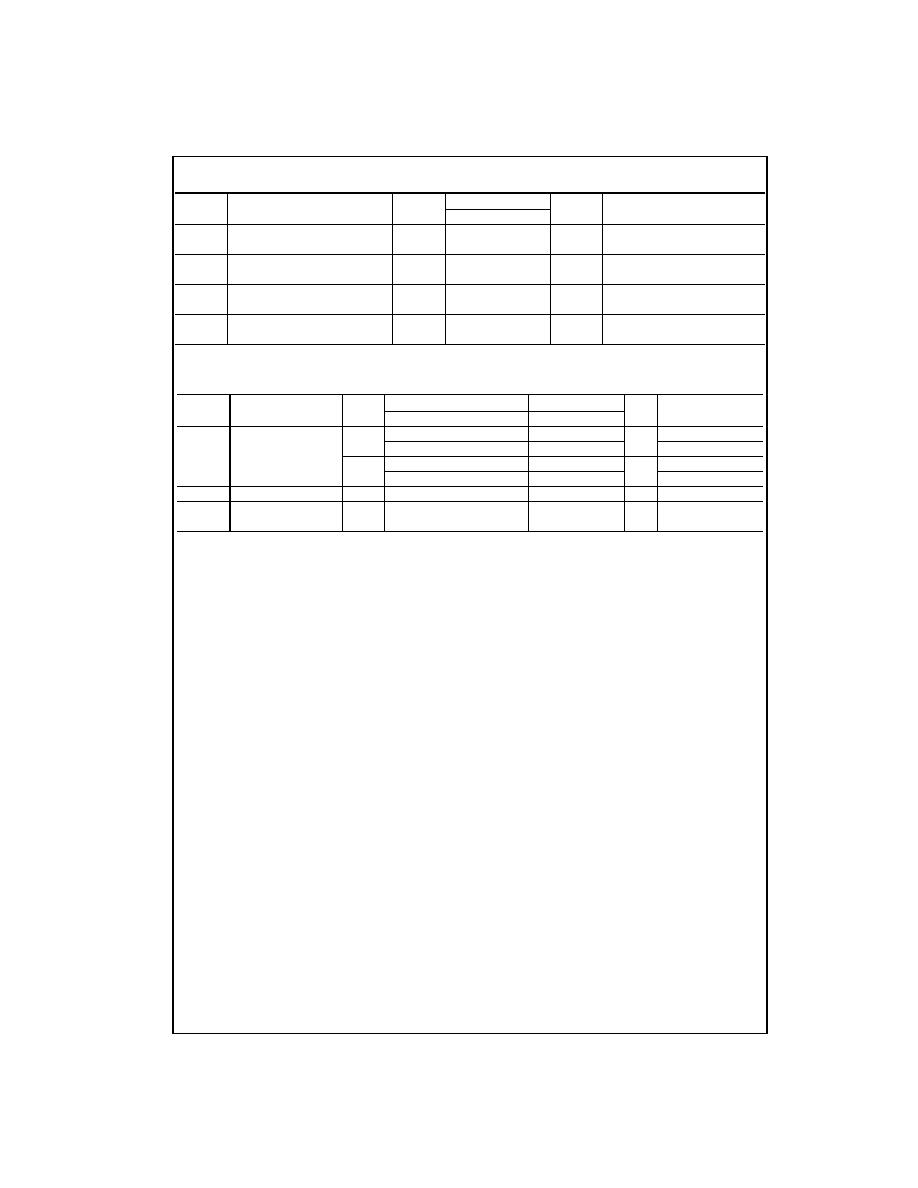
Absolute Maximum Ratings
(Note 2)
Recommended Operating
Conditions
(Note 3)
Note 2: Absolute Maximum Ratings are values beyond which the device
may be damaged or have its useful life impaired. The databook specifica-
tions should be met, without exception, to ensure that the system design is
reliable over its power supply, temperature, and output/input loading vari-
ables. Fairchild does not recommend operation outside databook specifica-
tions.
Note 3: Unused inputs must be held HIGH or LOW. They may not float.
DC Electrical Characteristics
Supply Voltage (V
CC
)
0.5V to
7.0V
DC Input Voltage (V
IN
)
0.5V to
7.0V
DC Output Voltage (V
OUT
)
0.5V to V
CC
0.5V
Input Diode Current (I
IK
)
20 mA
Output Diode Current (I
OK
)
r
20 mA
DC Output Current (I
OUT
)
r
25 mA
DC V
CC
/GND Current (I
CC
)
r
50 mA
Storage Temperature (T
STG
)
65
q
C to
150
q
C
Lead Temperature (T
L
)
(Soldering, 10 seconds)
260
q
C
Supply Voltage (V
CC
)
2.0V to
5.5V
Input Voltage (V
IN
)
0V to
5.5V
Output Voltage (V
OUT
)
0V to V
CC
Operating Temperature (T
OPR
)
40
q
C to
85
q
C
Symbol
Parameter
V
CC
(V)
T
A
25
q
C
T
A
40
q
C to
85
q
C
Units
Conditions
Min
Typ
Max
Min
Max
V
P
Positive
3.0
2.20
2.20
V
Threshold Voltage
4.5
3.15
3.15
5.5
3.85
3.85
V
N
Negative
3.0
0.90
0.90
V
Threshold Voltage
4.5
1.35
1.35
5.5
1.65
1.65
V
H
Hysteresis
3.0
0.30
1.20
0.30
1.20
V
Output Voltage
4.5
0.40
1.40
0.40
1.40
5.5
0.50
1.60
0.50
1.60
V
OH
HIGH Level
2.0
1.9
2.0
1.9
V
IN
V
IH
I
OH
50
P
A
Output Voltage
3.0
2.9
3.0
2.9
V
or V
IL
4.5
4.4
4.5
4.4
3.0
2.58
2.48
V
I
OH
4 mA
4.5
3.94
3.80
I
OH
8 mA
V
OL
LOW Level
2.0
0.0
0.1
0.1
V
IN
V
IH
I
OL
50
P
A
Output Voltage
3.0
0.0
0.1
0.1
V
or V
IL
4.5
0.0
0.1
0.1
3.0
0.36
0.44
V
I
OL
4 mA
4.5
0.36
0.44
I
OL
8 mA
I
IN
Input Leakage Current
0≠5.5
r
0.1
r
1.0
P
A
V
IN
5.5V or GND
I
CC
Quiescent Supply Current
5.5
2.0
20.0
P
A
V
IN
V
CC
or GND
www.fairchildsemi.com
4
74
V
HC132
Noise Characteristics
Note 4: Parameter guaranteed by design
AC Electrical Characteristics
Note 5: C
PD
is defined as the value of the internal equivalent capacitance which is calculated from the operating current consumption without load. Average
operating current can be obtained from the equation: I
CC
(opr.)
C
PD
* V
CC
* I
IN
I
CC
/4 (per gate)
Symbol
Parameter
V
CC
(V)
T
A
25
q
C
Units
Conditions
Typ
Limit
V
OLP
Quiet Output Maximum
5.0
0.3
0.8
V
C
L
50 pF
(Note 4)
Dynamic V
OL
V
OLV
Quiet Output Maximum
5.0
0.3
0.8
V
C
L
50 pF
(Note 4)
Dynamic V
OL
V
IHD
Maximum HIGH Level
5.0
3.5
V
C
L
50 pF
(Note 4)
Dynamic Input Voltage
V
ILD
Maximum
LOW
Level
5.0
1.5
V
C
L
50 pF
(Note 4)
Dynamic Input Voltage
Symbol
Parameter
V
CC
(V)
T
A
25
q
C
T
A
40
q
C to
85
q
C
Units
Conditions
Min
Typ
Max
Min
Max
t
PHL
Propagation Delay
3.3
r
0.3
6.1
11.9
1.0
14.0
ns
C
L
15 pF
t
PLH
8.0
15.4
1.0
17.5
C
L
50 pF
5.0
r
0.5
3.9
7.7
1.0
9.0
ns
C
L
15 pF
5.9
9.7
1.0
11.0
C
L
50 pF
C
IN
Input Capacitance
4
10
10
pF
V
CC
Open
C
PD
Power Dissipation
16
pF
(Note 5)
Capacitance

5
www.fairchildsemi.com
7
4
VH
C13
2
Physical Dimensions
inches (millimeters) unless otherwise noted
14-Lead Small Outline Integrated Circuit (SOIC), JEDEC MS-012, 0.150" Narrow
Package Number M14A

www.fairchildsemi.com
6
74
V
HC132
Physical Dimensions
inches (millimeters) unless otherwise noted (Continued)
Pb-Free 14-Lead Small Outline Package (SOP), EIAJ TYPE II, 5.3mm Wide
Package Number M14D

7
www.fairchildsemi.com
7
4
VH
C13
2
Physical Dimensions
inches (millimeters) unless otherwise noted (Continued)
14-Lead Thin Shrink Small Outline Package (TSSOP), JEDEC MO-153, 4.4mm Wide
Package Number MTC14

www.fairchildsemi.com
8
74
V
HC132
Quad 2-I
nput NAND
Schmit
t T
r
i
gger
Physical Dimensions
inches (millimeters) unless otherwise noted (Continued)
14-Lead Plastic Dual-In-Line Package (PDIP), JEDEC MS-001, 0.300" Wide
Package Number N14A
Fairchild does not assume any responsibility for use of any circuitry described, no circuit patent licenses are implied and
Fairchild reserves the right at any time without notice to change said circuitry and specifications.
LIFE SUPPORT POLICY
FAIRCHILD'S PRODUCTS ARE NOT AUTHORIZED FOR USE AS CRITICAL COMPONENTS IN LIFE SUPPORT
DEVICES OR SYSTEMS WITHOUT THE EXPRESS WRITTEN APPROVAL OF THE PRESIDENT OF FAIRCHILD
SEMICONDUCTOR CORPORATION. As used herein:
1. Life support devices or systems are devices or systems
which, (a) are intended for surgical implant into the
body, or (b) support or sustain life, and (c) whose failure
to perform when properly used in accordance with
instructions for use provided in the labeling, can be rea-
sonably expected to result in a significant injury to the
user.
2. A critical component in any component of a life support
device or system whose failure to perform can be rea-
sonably expected to cause the failure of the life support
device or system, or to affect its safety or effectiveness.
www.fairchildsemi.com