© 2005 Fairchild Semiconductor Corporation
DS011520
www.fairchildsemi.com
November 1992
Revised April 2005
7
4
VH
C24
5
Oct
a
l
Bi
dir
ecti
onal
T
r
anscei
ver
wit
h
3-
ST
A
T
E
Output
s
74VHC245
Octal Bidirectional Transceiver with 3-STATE Outputs
General Description
The VHC245 is an advanced high speed CMOS octal bus
transceiver fabricated with silicon gate CMOS technology.
It achieves high speed operation similar to equivalent Bipo-
lar Schottky TTL while maintaining the CMOS low power
dissipation. The VHC245 is intended for bidirectional asyn-
chronous communication between data busses. The direc-
tion of data transmission is determined by the level of the
T/R input. The enable input can be used to disable the
device so that the busses are effectively isolated. All inputs
are equipped with protection circuits against static dis-
charge.
Features
s
High Speed: t
PD
4.0 ns (typ) at V
CC
5V
s
High Noise Immunity: V
NIH
V
NIL
28% V
CC
(Min)
s
Power Down Protection is provided on all inputs
s
Low Noise: V
OLP
0.9V (typ)
s
Low Power Dissipation:
I
CC
4
P
A (Max) @ T
A
25
q
C
s
Pin and Function Compatible with 74HC245
Ordering Code:
Surface mount packages are also available on Tape and Reel. Specify by appending the suffix letter "X" to the ordering code.
Pb-Free package per JEDEC J-STD-020B.
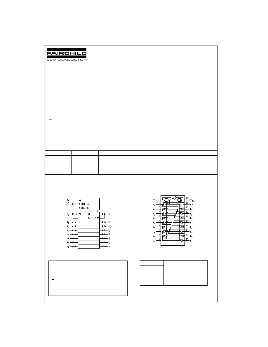
Logic Symbol
IEEE/IEC
Pin Description
Connection Diagram
Truth Table
H
HIGH Voltage Level
L
LOW Voltage Level
X
Immaterial
Any unused bus terminals during HIGH-Z State must be held HIGH or
LOW.
Order Number
Package Number
Package Description
74VHC245M
M20B
20-Lead Small Outline Integrated Circuit (SOIC), JEDEC MS-013, 0.300" Wide
74VHC245SJ
M20D
Pb-Free 20-Lead Small Outline Package (SOP), EIAJ TYPE II, 5.3mm Wide
74VHC245MTC
MTC20
20-Lead Thin Shrink Small Outline Package (TSSOP), JEDEC MO-153, 4.4mm Wide
74VHC245N
N20A
20-Lead Plastic Dual-In-Line Package (PDIP), JEDEC MS-001, 0.300" Wide
Pin
Description
Names
OE
Output Enable Input
T/R
Transmit/Receive Input
A
0
≠A
7
Side A Inputs or 3-STATE Outputs
B
0
≠B
7
Side B Inputs or 3-STATE Outputs
Inputs
Outputs
OE
T/R
L
L
Bus B Data to Bus A
L
H
Bus A Data to Bus B
H
X
HIGH-Z State

www.fairchildsemi.com
2
74
V
HC245
Absolute Maximum Ratings
(Note 1)
Recommended Operating
Conditions
(Note 2)
Note 1: Absolute Maximum Ratings are values beyond which the device
may be damaged or have its useful life impaired. The databook specifica-
tions should be met, without exception, to ensure that the system design is
reliable over its power supply, temperature, and output/input loading vari-
ables. Fairchild does not recommend operation outside databook specifica-
tions.
Note 2: Unused inputs or I/O pins must be held HIGH or LOW. They may
not float.
DC Electrical Characteristics
Supply Voltage (V
CC
)
0.5V to
7.0V
DC Input Voltage (V
IN
) (T/R, OE)
0.5V to 7.0V
DC Output Voltage (V
OUT
)
0.5V to V
CC
0.5V
Input Diode Current (I
IK
) (T/R, OE)
20 mA
Output Diode Current (I
OK
)
r
20 mA
DC Output Current (I
OUT
)
r
25 mA
DC V
CC
/GND Current (I
CC
)
r
75 mA
Storage Temperature (T
STG
)
65
q
C to
150
q
C
Lead Temperature (T
L
)
(Soldering, 10 seconds)
260
q
C
Supply Voltage (V
CC
)
2.0V to 5.5V
Input Voltage (V
IN
)(T/R, OE)
0V to 5.5V
Output Voltage (V
OUT
)
0V to V
CC
Operating Temperature (T
OPR
)
40
q
C to
85
q
C
Input Rise and Fall Time (t
r
, t
f
)
V
CC
3.3V
r
0.3V
0
a
100 ns/V
V
CC
5.0V
r
0.5V
0
a
20 ns/V
Symbol
Parameter
V
CC
T
A
25
q
C
T
A
40
q
C to
85
q
C
Units
Conditions
(V)
Min
Typ
Max
Min
Max
V
IH
HIGH Level
2.0
1.50
1.50
V
Input Voltage
3.0
5.5
0.7 V
CC
0.7 V
CC
V
IL
LOW Level
2.0
0.50
0.50
V
Input Voltage
3.0
5.5
0.3 V
CC
0.3 V
CC
V
OH
HIGH Level
2.0
1.9
2.0
1.9
V
IN
V
IH
I
OH
50
P
A
Output Voltage
3.0
2.9
3.0
2.9
V
or V
IL
4.5
4.4
4.5
4.4
3.0
2.58
2.48
V
I
OH
4 mA
4.5
3.94
3.80
I
OH
8 mA
V
OL
LOW Level
2.0
0.0
0.1
0.1
V
IN
V
IH
I
OL
50
P
A
Output Voltage
3.0
0.0
0.1
0.1
V
or V
IL
4.5
0.0
0.1
0.1
3.0
0.36
0.44
V
I
OL
4 mA
4.5
0.36
0.44
I
OL
8 mA
I
OZ
3-STATE Output
V
IN
V
CC
or GND
Off-State Current
5.5
r
0.25
r
2.5
P
A
V
OUT
V
CC
or GND
V
IN
OE
V
IH
or V
IL
I
IN
Input Leakage
0
5.5
r
0.1
r
1.0
P
A
V
IN
5.5V or GND
(T/R, OE)
Current
I
CC
Quiescent Supply Current
5.5
4.0
40.0
P
A
V
IN
V
CC
or GND

3
www.fairchildsemi.com
7
4
VH
C24
5
Noise Characteristics
Note 3: Parameter guaranteed by design.
AC Electrical Characteristics
Note 4: Parameter guaranteed by design. t
OSLH
|t
PLH max
t
PLH min
|; t
OSHL
|t
PHL max
t
PHL min
|
Note 5: C
PD
is defined as the value of the internal equivalent capacitance which is calculated from the operating current consumption without load. Average
operating current can be obtained by the equation: I
CC
(opr.)
C
PD
* V
CC
* f
IN
I
CC
/8 (per Bit).
Symbol
Parameter
V
CC
T
A
25
q
C
Units
Conditions
(V)
Typ
Limits
V
OLP
Quiet Output Maximum
5.0
0.9
1.2
V
C
L
50 pF
(Note 3)
Dynamic V
OL
V
OLV
Quiet Output Minimum
5.0
0.9
1.2
V
C
L
50 pF
(Note 3)
Dynamic V
OL
V
IHD
Minimum HIGH Level
5.0
3.5
V
C
L
50 pF
(Note 3)
Dynamic Input Voltage
V
ILD
Maximum LOW Level
5.0
1.5
V
C
L
50 pF
(Note 3)
Dynamic Input Voltage
Symbol
Parameter
V
CC
T
A
25
q
C
T
A
40
q
C to
85
q
C
Units
Conditions
(V)
Min
Typ
Max
Min
Max
t
PLH
Propagation Delay
3.3
r
0.3
5.8
8.4
1.0
10.0
ns
C
L
15 pF
t
PHL
Time
8.3
11.9
1.0
13.5
C
L
50 pF
5.0
r
0.5
4.0
5.5
1.0
6.5
ns
C
L
15 pF
5.5
7.5
1.0
8.5
C
L
50 pF
t
PZL
3-STATE Output
3.3
r
0.3
8.5
13.2
1.0
15.5
ns
R
L
1 k
:
C
L
15 pF
t
PZH
Enable Time
11.0
16.7
1.0
19.0
C
L
50 pF
5.0
r
0.5
5.8
8.5
1.0
10.0
ns
C
L
15 pF
7.3
10.6
1.0
12.0
C
L
50 pF
t
PLZ
3-STATE Output
3.3
r
0.3
11.5
15.8
1.0
18.0
ns
R
L
1 k
:
C
L
50 pF
t
PHZ
Disable Time
5.0
r
0.5
7.0
9.7
1.0
11.0
C
L
50 pF
t
OSLH
Output to Output
3.3
r
0.3
1.5
1.5
ns
(Note 4)
C
L
50 pF
t
OSHL
Skew
5.0
r
0.5
1.0
1.0
C
L
50 pF
C
IN
Input Capacitance
4
10
10
pF
V
CC
Open
(T/R, OE)
C
I/O
Output Capacitance
8
pF
V
CC
5.0V
C
PD
Power Dissipation
21
pF
(Note 5)
Capacitance

www.fairchildsemi.com
4
74
V
HC245
Physical Dimensions
inches (millimeters) unless otherwise noted
20-Lead Small Outline Integrated Circuit (SOIC), JEDEC MS-013, 0.300" Wide
Package Number M20B

5
www.fairchildsemi.com
7
4
VH
C24
5
Physical Dimensions
inches (millimeters) unless otherwise noted (Continued)
Pb-Free 20-Lead Small Outline Package (SOP), EIAJ TYPE II, 5.3mm Wide
Package Number M20D