© 2005 Fairchild Semiconductor Corporation
DS500025
www.fairchildsemi.com
July 1997
Revised February 2005
7
4
VH
CT0
8
A
Quad 2-I
nput AND
Gat
e
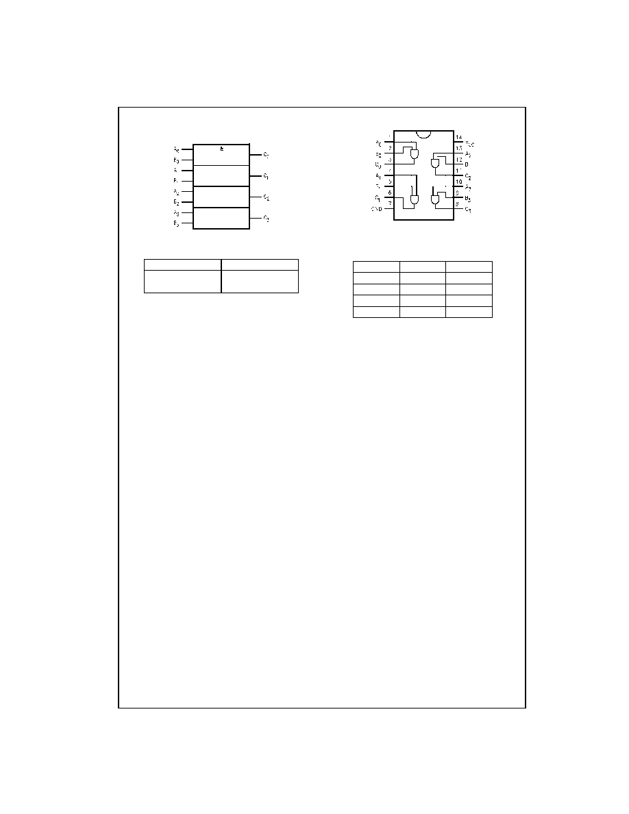
74VHCT08A
Quad 2-Input AND Gate
General Description
The VHCT08A is an advanced high speed CMOS 2 Input
AND Gate fabricated with silicon gate CMOS technology. It
achieves the high-speed operation similar to equivalent
Bipolar Schottky TTL while maintaining the CMOS low
power dissipation.
The internal circuit is composed of 4 stages including buffer
output, which provide high noise immunity and stable out-
put.
Protection circuits ensure that 0V to 7V can be applied to
the input pins without regard to the supply voltage and to
the output pins with V
CC
0V. These circuits prevent
device destruction due to mismatched supply and input/
output voltages. This device can be used to interface 3V to
5V systems and two supply systems such as battery
backup.
Features
s
High speed: t
PD
5.0 ns (typ) at T
A
25
q
C
s
High noise immunity: V
IH
2.0V, V
IL
0.8V
s
Power down protection is provided on all inputs and
outputs
s
Low noise: V
OLP
0.8V (max)
s
Low power dissipation:
I
CC
2
P
A (max) @ T
A
25
q
C
s
Pin and function compatible with 74HCT08
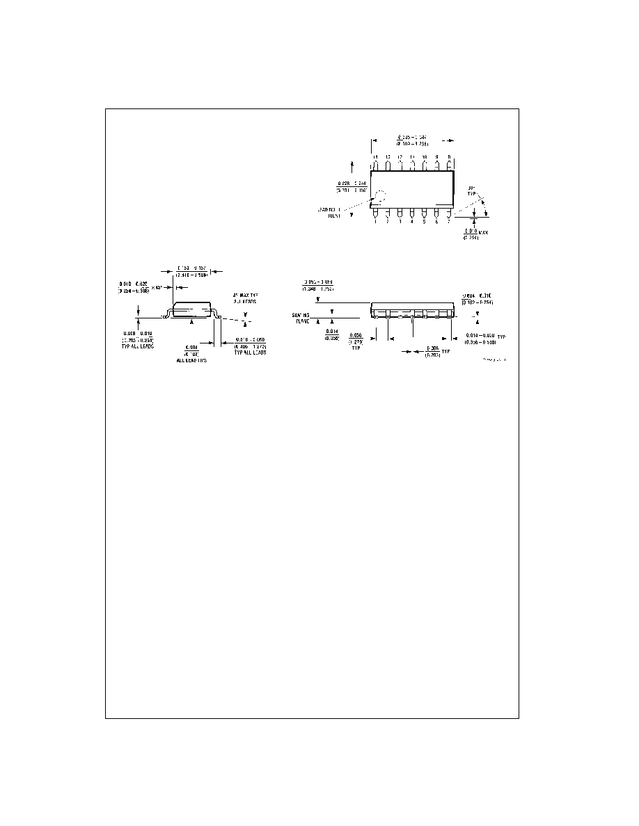
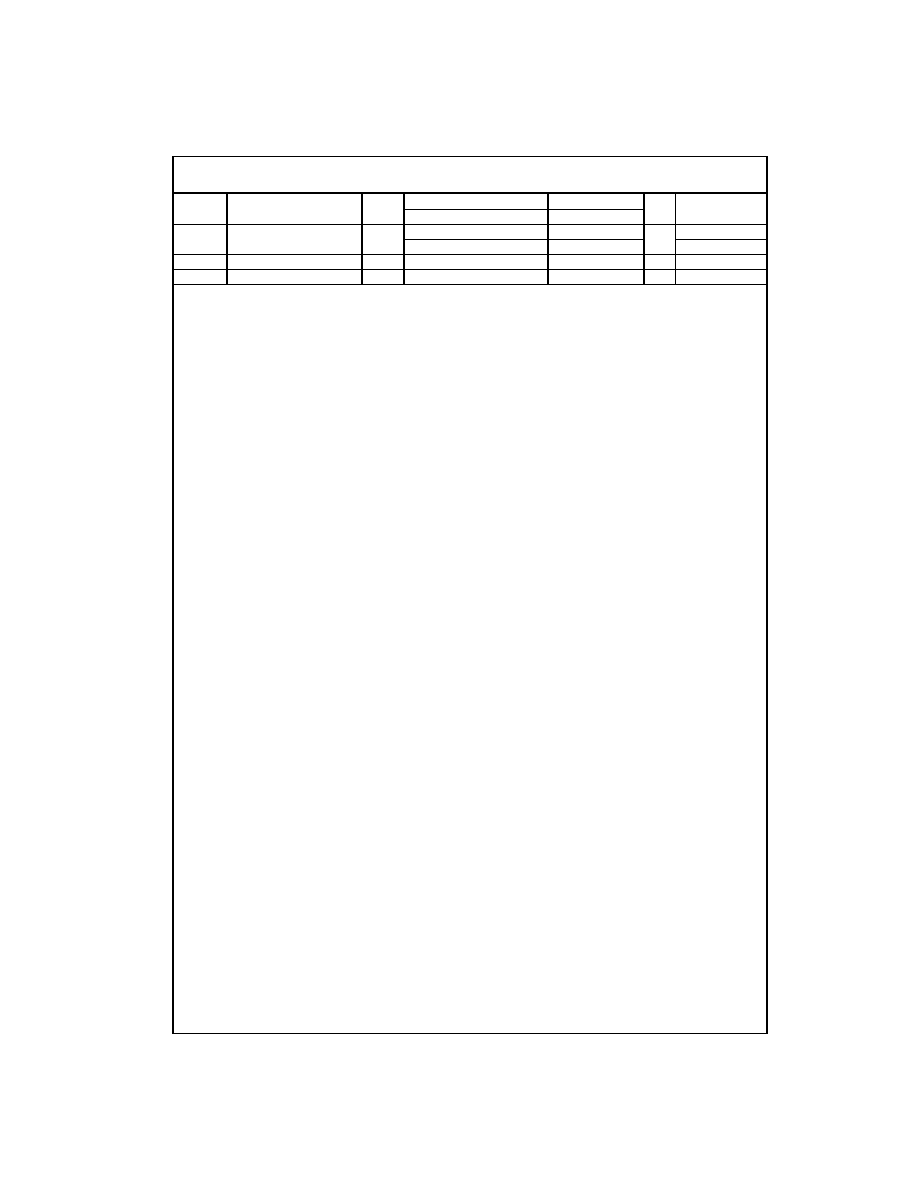
Ordering Code:
Surface mount packages are also available on Tape and Reel. Specify by appending the suffix letter "X" to the ordering code
Pb-Free package per JEDEC J-STD-020B.
Note 1: "_NL" indicates Pb-Free package (per JEDEC J-STD-020B). Device available in Tape and Reel only.
Order Number
Package
Package Description
Number
74VHCT08AM
M14A
14-Lead Small Outline Integrated Circuit (SOIC), JEDEC MS-012, 0.150" Narrow
74VHCT08AMX_NL
(Note 1)
M14A
Pb-Free 14-Lead Small Outline Integrated Circuit (SOIC), JEDEC MS-012, 0.150" Narrow
74VHCT08ASJ
M14D
Pb-Free 14-Lead Small Outline Package (SOP), EIAJ TYPE II, 5.3mm Wide
74VHCT08AMTC
MTC14
14-Lead Thin Shrink Small Outline Package (TSSOP), JEDEC MO-153, 4.4mm Wide
74VHCT08AMTCX_NL
(Note 1)
MTC14
Pb-Free 14-Lead Thin Shrink Small Outline Package (TSSOP), JEDEC MO-153, 4.4mm
Wide
74VHCT08AN
N14A
14-Lead Plastic Dual-In-Line Package (PDIP), JEDEC MS-001, 0.300" Wide
3
www.fairchildsemi.com
7
4
VH
CT0
8
A
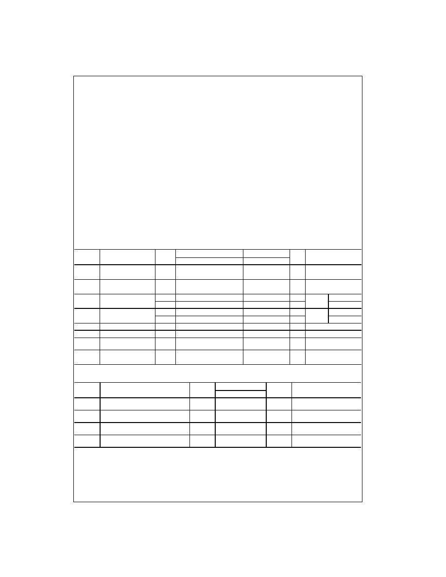
Absolute Maximum Ratings
(Note 2)
Recommended Operating
Conditions
(Note 6)
Note 2: Absolute Maximum Ratings are values beyond which the device
may be damaged or have its useful life impaired. The databook specifica-
tions should be met, without exception, to ensure that the system design is
reliable over its power supply, temperature, and output/input loading vari-
ables. Fairchild does not recommend operation outside databook specifica-
tions.
Note 3: HIGH or LOW state. I
OUT
absolute maximum rating must be
observed.
Note 4: V
CC
0V.
Note 5: V
OUT
GND, V
OUT
!
V
CC
(Outputs Active).
Note 6: Unused inputs must be held HIGH or LOW. They may not float.
DC Electrical Characteristics
Noise Characteristics
Note 7: Parameter guaranteed by design.
Supply Voltage (V
CC
)
0.5V to
7.0V
DC Input Voltage (V
IN
)
0.5V to
7.0V
DC Output Voltage (V
OUT
)
(Note
3)
0.5V to V
CC
0.5V
(Note
4)
0.5V to 7.0V
Input Diode Current (I
IK
)
20 mA
Output Diode Current (I
OK
) (Note 5)
r
20 mA
DC Output Current (I
OUT
)
r
25 mA
DC V
CC
/GND Current (I
CC
)
r
50 mA
Storage Temperature (T
STG
)
65
q
C to
150
q
C
Lead Temperature (T
L
)
(Soldering, 10 seconds)
260
q
C
Supply Voltage (V
CC
)
4.5V to 5.5V
Input Voltage (V
IN
)
0V to
5.5V
Output Voltage (V
OUT
)
(Note 3)
0V to V
CC
(Note 4)
0V to 5.5V
Operating Temperature (T
OPR
)
40
q
C to
85
q
C
Input Rise and Fall Time (t
r
, t
f
)
V
CC
5.0V
r
0.5V
0 ns/V
a
20 ns/V
Symbol
Parameter
V
CC
(V)
T
A
25
q
C
T
A
40
q
C to
85
q
C
Units
Conditions
Min
Typ
Max
Min
Max
V
IH
HIGH Level
4.5
2.0
2.0
V
Input Voltage
5.5
2.0
2.0
V
IL
LOW Level
4.5
0.8
0.8
V
Input Voltage
5.5
0.8
0.8
V
OH
HIGH Level
4.5
4.40
4.50
4.40
V
V
IN
V
IH
or V
IL
I
OH
50
P
A
Output Voltage
4.5
3.94
3.80
V
I
OH
8 mA
V
OL
LOW Level Output Voltage
4.5
0.0
0.1
0.1
V
V
IN
V
IH
or V
IL
I
OL
50
P
A
4.5
0.36
0.44
V
I
OL
8 mA
I
IN
Input Leakage Current
0
5.5
r
0.1
r
1.0
P
A
V
IN
5.5V or GND
I
CC
Quiescent Supply Current
5.5
2.0
20.0
P
A
V
IN
V
CC
or GND
I
CCT
Maximum I
CC
/ Input
5.5
1.35
1.50
mA
V
IN
3.4V
Other Inputs
V
CC
or GND
I
OFF
Output Leakage Current
0.0
0.5
5.0
P
A
V
OUT
5.5V
(Power Down State)
Symbol
Parameter
V
CC
(V)
T
A
25
q
C
Units
Conditions
Typ
Limit
V
OLP
(Note 7)
Quiet Output Maximum Dynamic V
OL
5.0
0.4
0.8
V
C
L
50 pF
V
OLV
(Note 7)
Quiet Output Minimum Dynamic V
OL
5.0
0.4
0.8
V
C
L
50 pF
V
IHD
(Note 7)
Minimum HIGH Level Dynamic Input Voltage
5.0
2.0
V
C
L
50 pF
V
ILD
(Note 7)
Maximum LOW Level Dynamic Input Voltage
5.0
0.8
V
C
L
50 pF
www.fairchildsemi.com
4
74VHC
T0
8A
AC Electrical Characteristics
Note 8: C
PD
is defined as the value of the internal equivalent capacitance, which is calculated from the operating current consumption without load. Average
operating current can be obtained from the equation: I
CC
(opr.)
C
PD
* V
CC
* f
IN
I
CC
/4 (per gate)
Symbol
Parameter
V
CC
(V)
T
A
25
q
C
T
A
40
q
C to
85
q
C
Units
Conditions
Min
Typ
Max
Min
Max
t
PLH
Propagation Delay
5.0
5.0
6.9
1.0
8.0
ns
C
L
15 pF
t
PHL
r
0.5
5.5
7.9
1.0
9.0
C
L
50 pF
C
IN
Input Capacitance
4
10
10
pF
V
CC
Open
C
PD
Power Dissipation Capacitance
18
pF
(Note 8)