 | ÐлекÑÑоннÑй компоненÑ: AN4129 | СкаÑаÑÑ:  PDF PDF  ZIP ZIP |
Äîêóìåíòàöèÿ è îïèñàíèÿ www.docs.chipfind.ru
Application Note AN4129
Green Current Mode PWM Controller FAN7601
www.fairchildsemi.com
©2003 Fairchild Semiconductor Corporation
1. Introduction
This application note describes the operation and features of
the FAN7601. This device is a BCDMOS programmable
frequency current mode PWM controller which is designed
for off-line adapter applications and auxiliary power
supplies. To reduce power loss at light and no load, the
FAN7601 operates in burst mode and it includes a start-up
switch to reduce the losses in the start-up circuit.
Because of the internal start-up switch and burst mode oper-
ation, it is possible to supply an output power of 0.5W with
under 1W input power when the input line voltage is 265V.
On no load condition, input power is under 0.3W.
The FAN7601 offers a latch protection pin for the protection
of the system e.g. over voltage protection and/or thermal
shutdown.
The internal over voltage protection function shuts down the
IC operation when the supply voltage reaches 19V.
In addition, a soft start function is provided, and the soft start
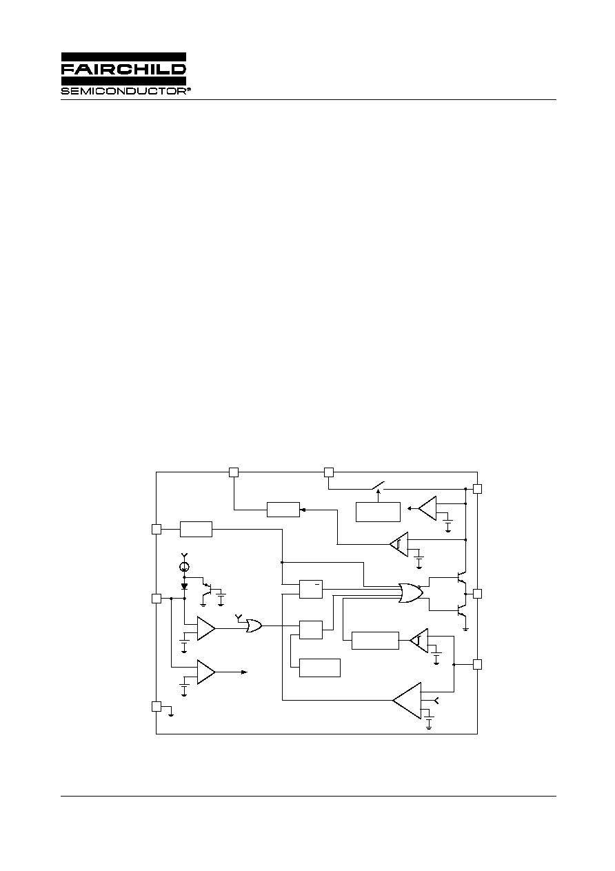
time can be varied. Figure 1 shows a block diagram for the
FAN7601.
It contains the following blocks.
· Start-up circuit and reference
· Oscillator
· Soft start and latch
· Current sense and feed back
· Burst mode
· Output drive
Rev. 1.0.1
Latch/SS
Delay Circuit
1V
Enable
+
-
-
GND
Start-up
Circuit
2.5V
1.5V
Start-up
Circuit
5V Ref
Vcc
Vref
Rt/Ct
Latch/SS
OUT
CS/FB
UVLO
12uA
Vref
7
19V
OVP
+
-
+
-
12V/8V
6
2
+
-
0.97V/0.9V
1
8
R
Q
S
OSC
4
3
+
-
OVP
R
Q
S
Reset
Circuit
+
-
5
Vstr
1V
Figure 1. Internal Block Diagram of the FAN7601
AN4129
APPLICATION NOTE
2
©2003 Fairchild Semiconductor Corporation
2. Device Block Description
1. Start-up Circuit And Reference
The FAN7601 contains a start-up switch to reduce power
loss in the external start-up circuit of conventional PWM
converters. The internal start-up circuit charges the Vcc
capacitor with a 1mA current source if the line is connected
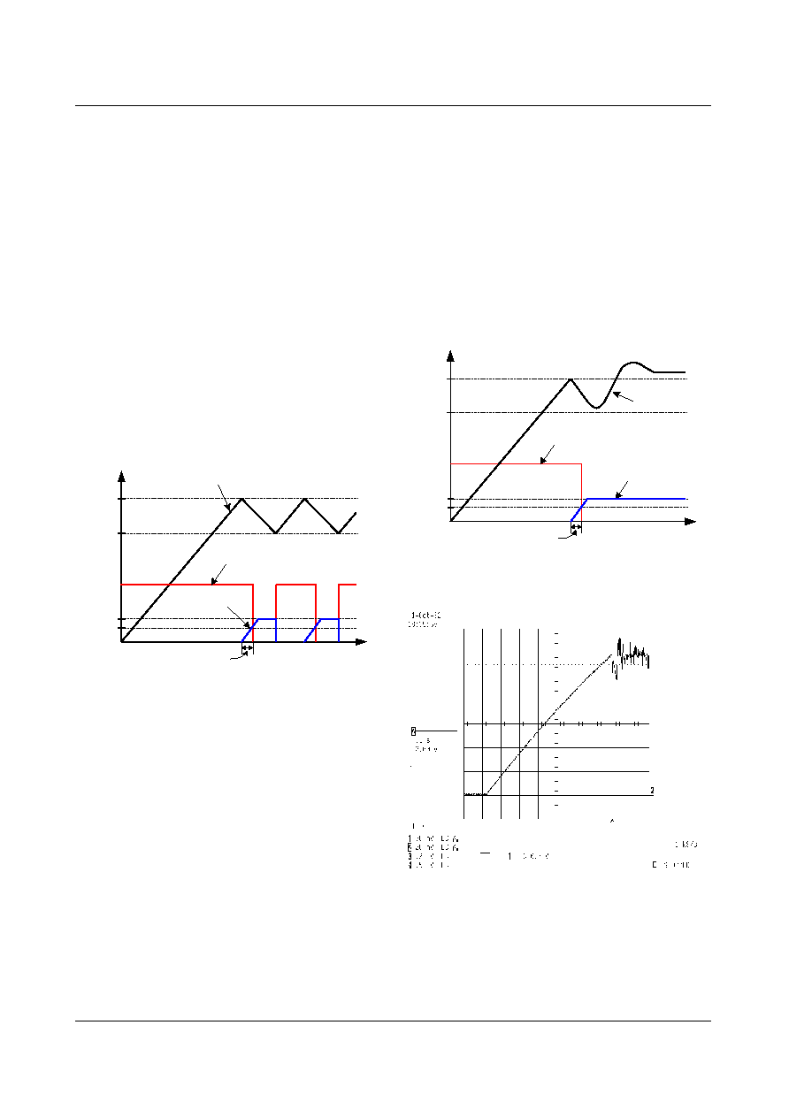
until the soft start is completed as shown in Fig. 2. The soft
start function starts when the Vcc voltage reaches the start
threshold voltage(typically 12V) and it ends when the
LATCH/SS pin voltage reaches 1V. The internal start-up
circuit starts charging the Vcc capacitor again if the Vcc
voltage is lowered to the minimum operating voltage
(typically 8V). In such a case the UVLO block shuts down
the output drive circuit and some other blocks to reduce the
IC current, and the soft start capacitor is discharged to zero
voltage. If the Vcc voltage reaches the start threshold volt-
age, the IC starts switching again and the soft start capacitor
is charged from zero voltage. The internal start-up circuit
supplies
current until the soft start is completed .
Figure 2. Start-up Current and Vcc Voltage
Figure 3 shows a typical start-up sequence for the FAN7601.
The Vcc voltage should be higher than the minimum
operating voltage at start-up to enter a steady state. If the
Vcc voltage is higher than 19V, the over voltage protection
function works. There is some delay in the over voltage
protection circuit. The Vcc capacitor can be selected
according to the soft start time and total gate charge(Qg) of
the MOSFET. In the data sheet, the operating supply current
is measured with a 1nF capacitor connected at the OUT pin.
Therefore the real operating current necessary for the IC
operation excluding the MOSFET drive is typically 2mA.
During the soft start period (Tss), the Vcc capacitor is
charged by a 1mA start-up current from the Vstr pin and the
Vcc capacitor is discharged by a 2mA IC operating current
and the MOSFET gate drive current. The MOSFET gate
drive current is Qg
×
fsw. Qg increases according to the MOS-
FET drain source voltage, therefore the drive current is max-
imum when the input line voltage is highest. During the soft
start period , the converter output voltage is very low, so few
current is supplied to the Vcc capacitor from the Vcc wind-
ing. Therefore the Vcc capacitor must be large enough to
supply sufficient current during the soft start time when
starting up. The value of the Vcc capacitor is determined by
(1) where 4V is the UVLO hysteresis and 2mA is the IC
operating current and 1mA is the start-up current.
Figure 4 shows the Vcc voltage when starting up with a 47uF
capacitor and a FQPF7N60 MOSFET. The input line voltage
is 265V and the soft start time is about 40ms.
Figure 3. Typical Start-up Sequence for FAN7601
Figure 4. Vcc Voltage Waveform at Start-up
The FAN7601 provides the Vref pin. The reference output
voltage is 5V. Because this voltage is the reference of the IC
operation, a 100nF ceramic capacitor must be connected
between the Vref pin and the GND pin to filter the switching
noise as close as possible to the IC.
Soft Start
Time
t
V
TH
V
TL
Vcc
Start-up
Current
Soft Start
Voltage
1V
1.5V
C
Vcc
Tss
2mA 1mA
Q
g
+
f
sw
(
)
4V
------------------------------------------------------------------------------
>
(1)
t
V
TH
V
TL
Vcc
Start-up
Current
Soft Start
Voltage
Soft Start
Time
1V
1.5V
APPLICATION NOTE
AN4129
3
©2003 Fairchild Semiconductor Corporation
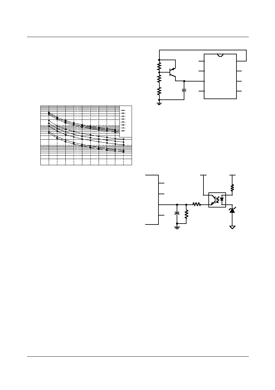
2. Oscillator
The oscillator frequency is programmed by selecting the
values of Rt and Ct. The capacitor Ct is charged from the 5V
reference through the resistor Rt to approximately 2.5V and
discharged to 1.25V by an internal current sink. Figure 5
shows the oscillator frequency characteristics according to
the variation of Rt and Ct. The values of Rt and Ct can be
chosen with reference to Fig. 5.
Figure 5. Oscillator Frequency Characteristics
3. Soft Start and Latch
The 12uA current source charges the soft start capacitor Css
when the Vcc voltage reaches the start threshold voltage.
The soft start ends when the Latch/SS pin voltage becomes
1V and the Latch/SS pin is charged up to 1.5V. The soft start
capacitor is reset when the Vcc voltage is lower than the
minimum operating voltage.
The soft start time Tss is calculated by (2).
Tss = Css/12
µ
A (2)
The latch protection is provided to protect the system.
The latch protection pin can be used for output over voltage
protection and/or thermal protection etc. If the Latch/SS pin
voltage is made greater than 2.5V by the external circuit,
then the IC is shut down. The latch protection is reset when
the Vcc voltage is lower than 5V.
Figure 6 shows a thermal protection circuit which uses an
NTC thermistor. As the temperature rises the resistance of
the NTC drops so the base voltage of the PNP transistor
drops. Then the PNP transistor turns on and charges the Css.
When the Latch/SS pin voltage is higher than 2.5V, the IC
goes to the shut down mode. The exact values of resistors
and NTC must be selected by an experiment because the
V
BE(sat)
of PNP
transistors and the leakage current of Css vary according to
the temperature.
Figure 6. Thermal Protection Circuit
Figure 7 shows an output over voltage protection circuit. If
the output voltage exceeds the sum of the zener diode
voltage and the photo coupler forward voltage drop, then the
capacitor Css is charged. In parallel with Css, a 1M
resistor
is connected because of the leakage
current of the photo coupler. If a 1M
is not connected the
leakage current of the photo coupler charges the Css up, and
the latch protection operates abnormally.
Figure 7. Output Over Voltage Protection Circuit
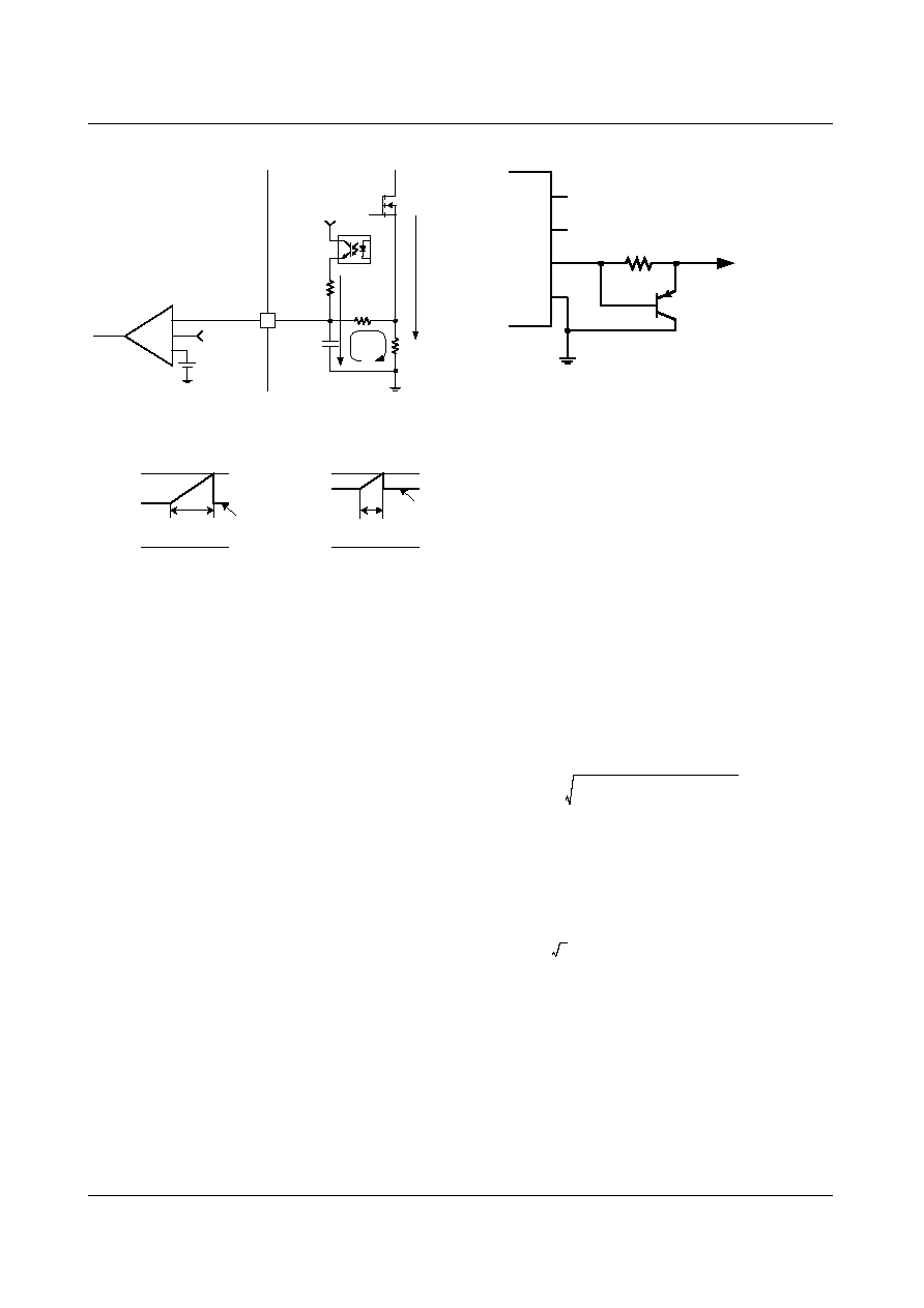
4. Current Sense and Feedback
The FAN7601 performs current sensing and output voltage
feedback with only one pin. To achieve the two functions
with one pin, an internal LEB(Leading Edge Blanking)
circuit for filtering current sensing noise is not included
because an external RC filter is necessary to add output
voltage feedback and current sensing information.
Figure 8 shows the current sensing and feedback circuits.
Rs is the current sensing resistor for sensing the switch
current. The current sensing information is filtered by an RC
filter composed of Rf and Cf. The current Ifb flowing
through the photo transistor varies according to the feedback
information and add an offset voltage on the sensed current
information as shown in Fig. 8 and Fig. 9. When the CS/FB
pin voltage touches 1V, the output drive circuit turns the
MOSFET off. The higher the DC offset is, the shorter the
switch-on time is. By varying the Ifb, the duty cycle is con-
0
10
20
30
40
50
1
10
100
1000
Ct=
680pF
820pF
1nF
2.2nF
3.3nF
4.7nF
8.2nF
10nF
F
r
equenc
y
(
k
Hz)
Rt (k
)
R1
NTC
R2
PNP
Css
5
6
7
8
Vref
Latch
/SS
1
2
3
4
Zener
Diode
1
2
3
4
Latch
/SS
1
2
3
4
Css
Vout
Vcc
1M
AN4129
APPLICATION NOTE
4
©2003 Fairchild Semiconductor Corporation
trolled.
Figure 8. Current Sensing and Feedback Circuit
Figure 9. CS/FB Pin Voltage Waveforms
5. Burst Mode
The FAN7601 contains a burst mode block to reduce power
loss at light and no load. A hysteresis comparator senses the
CS/FB offset voltage for the burst mode. The FAN7601
enters burst mode when the offset voltage of the CS/FB pin
is higher than 0.97V and exits the burst mode while the off-
set voltage is lower than 0.9V. The offset voltage is sensed
during the switch-off time. In the burst mod block, there are
about 4~8 switching cycles delay to filter the noise. By this
burst mode, a power consumption of less than 1W can be
achieved in standby mode.
6. Output Drive
The FAN7601 contains a single totem-pole output stage,
designed specifically for a direct drive of a power MOSFET.
The drive output is capable of up to 100mA peak current
with typical rise and fall times of 45ns, 35ns respectively
with a 1.0nF load. Additional circuitry has been added to
keep the drive output in a sinking mode whenever the UVLO
is active. This characteristic eliminates the need for an
external gate pull-down resistor.
The output drive capability can be improved by adding one
PNP bipolar transistor as shown in Fig. 10. In general, the
on-resistance is high to prevent voltage spike at turn-on, only
the turn-off characteristic is improved.
Figure 10. Circuit for Improving the Turn-Off
Characteristic
3. Design Example
A 50W adapter is designed to illustrate the design procedure.
The system parameters are as follows.
-
Maximum output power(Po) : 50W
-
Input voltage range : 85Vrms~265Vrms
-
Output voltage(Vo) : 12.1V
-
AC line frequency(fac) : 60Hz
-
Adapter efficiency(
) : > 80%
-
Switching frequency(fsw) : 91kHz
1. DC Link Capacitor and Bridge Diode
The DC link voltage becomes minimum when the output
power is maximum and input line voltage is lowest. The
minimum DC link voltage can be calculated using (3).
If the minimum voltage is chosen then the capacitance can
be calculated by (4).
If we choose the minimum voltage to be 70% of the peak
line voltage(
) then Cdc must be larger than 142uF.
The selected value is 150uF.
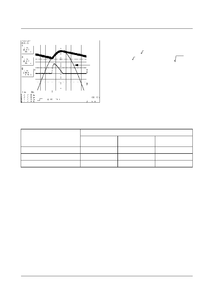
Figure 11 shows an experimental result for a 50W demo
board with a 150uF capacitor. Because the measured
efficiency is 84%, the minimum voltage is about 90V.
Latch/SS
1V
+
-
-
CS/FB
3
Current Sense
Comparator
Vcc
Cf
Rf
Rs
Rfb
Ifb
Isw
1V
CS/FB
GND
1V
CS/FB
GND
On Time
On Time
DC
Offset
DC
Offset
(a) Heavy Load Condition
(b) Light Load Condition
Out
8
7
6
5
PN2907
To MOSFET Gat
Vdc_min
2 Vac_min
2
Po_max
Cdc fac
--------------------------------
=
(3)
Cdc
Po_max
fac
2Vac_min
2
Vdc_min
2
(
)
--------------------------------------------------------------------------------------------
>
(4)
2 85V
APPLICATION NOTE
AN4129
5
©2003 Fairchild Semiconductor Corporation
Figure 11. DC Link Voltage and Current Waveforms
The bridge diode conduction time can be calculated by (5)
and the diode RMS current can be calculated by (6).
The calculated value is 1.3A and the selected bridge diode is
KBP206(600V/2A).
2. Transformer Design
Since 2001, the European Commission has been regulating
no load losses for AC adapters, battery chargers and
external power supplies under 75W.
Table 1 shows the regulation target specification.
Vdc_link
Vac
Iac
tc
1
2
fac
--------------------
=
arc
Vdc_min
2 Vac_min
--------------------------------------
cos
×
(5)
IBD RMS
(
)
2
=
2 Vac_min
Vdc_min
(
)
Cdc
2 fac
3 tc
----------------
(6)
Table 1:
European Commission Regulation Specification
Rated Input Power
No Load Power Consumption
Phase 1
1.1.2001
Phase 2
1.1.2003
Phase 3
1.1.2005
0.3W and < 15W
1.0W
0.75W
0.30W
15W and < 50W
1.0W
0.75W
0.50W
50W and < 75W
1.0W
0.75W
0.75W
At light and no load, the FAN7601 operates in burst mode to
reduce the power loss. To meet the regulation specification
the most important thing is to minimize the number of
MOSFET switchings. The flyback converter transfers energy
during the switch-off time. As the primary inductance of the
flyback transformer increases, the energy transferred to the
secondary side increases during one switching cycle. There-
fore it is better to use a higher inductance transformer, but
inductance is restricted by the size and cost of the trans-
former. In this design example, a 600uH transformer is
selected and the ferrite core is EER2828. The transformer
turns ratio is calculated when the input line voltage is lowest
and the output power is maximum. The maximum duty ratio
must be lower than 0.45 to prevent subharmonic oscillation.
In this design example, the turns ratio must be higher than
0.174 by (7).
Once the minimum turns ratio is determined, then the
numbers of primary and secondary turns is calculated when
input line voltage is highest and the output power is
maximum. If the converter operates in the CCM (Continuous
Conduction Mode) then the turn-on time can be calculated
by (8).
Then the number of primary turns can be obtained as in (9).
Ae is the effective cross sectional area of the core and Bmax
is the maximum flux density. Ae of EER2828 is 82.1mm
2
and Bmax is 0.15T. The calculated number of primary turns
is 54. Then the number of secondary turns can be calculated
by (10). The calculated number of secondary turns is 10.
The air gap length can be calculated by (11).
If the primary inductance is not high enough, the converter
can operate in the DCM(Discontinuous Conduction Mode)
when the input line voltage is highest and the output power is
maximum. For the DCM, the turn-on time can be calculated
as in (12).
n
1
D
max
D
max
-----------------------
>
Vo V
Diode
+
Vdc_min
--------------------------------
(7)
t
on
Vo V
Diode
+
n Vdc_max
Vo V
Diode
+
+
-------------------------------------------------------------------------
=
1
fsw
---------
(8)
Np
Vdc_max t
on
Ae Bmax
---------------------------------------
=
(9)
Ns
Np
=
Vo V
Diode
+
Vdc_min
--------------------------------
1 D
max
D
max
-----------------------
(10)
l
g
4
=
10
7
Ae
N
2
P
L
----------
(11)