
October 1987
Revised January 1999
CD401
06BC
He
x Sc
hmit
t T
r
ig
g
e
r
© 1999 Fairchild Semiconductor Corporation
DS005985.prf
www.fairchildsemi.com
CD40106BC
Hex Schmitt Trigger
General Description
The CD40106BC Hex Schmitt Trigger is a monolithic com-
plementary MOS (CMOS) integrated circuit constructed
with N and P-channel enhancement transistors. The posi-
tive and negative-going threshold voltages, V
T
+
and V
T
-
,
show low variation with respect to temperature (typ
0.0005V/
∞
C at V
DD
=
10V), and hysteresis, V
T
+
-
V
T
-
0.2
V
DD
is guaranteed.
All inputs are protected from damage due to static dis-
charge by diode clamps to V
DD
and V
SS
.
Features
s
Wide supply voltage range:
3V to 15V
s
High noise immunity:
0.7 V
DD
(typ.)
s
Low power TTL compatibility:
Fan out of 2 driving 74L or 1 driving 74LS
s
Hysteresis:
0.4 V
DD
(typ.),
0.2 V
DD
guaranteed
s
Equivalent to MM74C14
s
Equivalent to MC14584B
Ordering Code:
Devices also available in Tape and Reel. Specify by appending the suffix letter "X" to the ordering code.
Connection Diagram
Pin Assignments for DIP and SOIC
Top View
Schematic Diagram
Order Number
Package Number
Package Description
CD40106BCM
M14A
14-Lead Small Outline integrated Circuit (SOIC), JEDEC MS-120, 0.150" Narrow Body
CD40106BCN
N14A
14-Lead Plastic Dual-In-Line Package (PDIP), JEDEC MS-001, 0.300" Wide

www.fairchildsemi.com
2
C
D
401
06BC
Absolute Maximum Ratings
(Note 1)
(Note 2)
Recommended Operating
Conditions
(Note 2)
Note 1: "Absolute Maximum Ratings" are those values beyond which the
safety of the device cannot be guaranteed. They are not meant to imply
that the devices should be operated at these limits. The table of "Recom-
mended Operating Conditions" and "Electrical Characteristics" provides
conditions for actual device operation.
Note 2: V
SS
=
0V unless otherwise specified.
DC Electrical Characteristics
(Note 3)
Note 3: I
OH
and I
OL
are tested one output at a time.
DC Supply Voltage (V
DD
)
-
0.5 to
+
18 V
DC
Input Voltage (V
IN
)
-
0.5 to V
DD
+
0.5 V
DC
Storage Temperature Range (T
S
)
-
65
∞
C to
+
150
∞
C
Power Dissipation (P
D
)
Dual-In-Line
700 mW
Small Outline
500 mW
Lead Temperature (T
L
)
(Soldering, 10 seconds)
260
∞
C
DC Supply Voltage (V
DD
)
3 to 15 V
DC
Input Voltage (V
IN
)
0 to V
DD
V
DC
Operating Temperature Range (T
A
)
-
40
∞
C to
+
85
∞
C
Symbol
Parameter
Conditions
-
40
∞
C
+
25
∞
C
+
85
∞
C
Units
Min
Max
Min
Typ
Max
Min
Max
I
DD
Quiescent Device Current
V
DD
=
5V
4.0
4.0
30
µ
A
V
DD
=
10V
8.0
8.0
60
µ
A
V
DD
=
15V
16.0
16.0
120
µ
A
V
OL
LOW Level Output
|I
O
|
<
1
µ
A
Voltage
V
DD
=
5V
0.05
0.05
0.05
V
V
DD
=
10V
0.05
0.05
0.05
V
V
DD
=
15V
0.05
0.05
0.05
V
V
OH
HIGH Level Output
|I
O
|
<
1
µ
A
Voltage
V
DD
=
5V
4.95
4.95
5
4.95
V
V
DD
=
10V
9.95
9.95
10
0.95
V
V
DD
=
15V
14.95
14.95
15
14.95
V
V
T
-
Negative-Going Threshold
V
DD
=
5V, V
O
=
4.5V
0.7
2.0
0.7
1.4
2.0
0.7
2.0
V
Voltage
V
DD
=
10V, V
O
=
9V
1.4
4.0
1.4
3.2
4.0
1.4
4.0
V
V
DD
=
15V, V
O
=
13.5V
2.1
6.0
2.1
5.0
6.0
2.1
6.0
V
V
T
+
Positive-Going Threshold
V
DD
=
5V, V
O
=
0.5V
3.0
4.3
3.0
3.6
4.3
3.0
4.3
V
Voltage
V
DD
=
10V, V
O
=
1V
6.0
8.6
6.0
6.8
8.6
6.0
8.6
V
V
DD
=
15V, V
O
=
1.5V
9.0
12.9
9.0
10.0
12.9
9.0
12.9
V
V
H
Hysteresis (V
T
+
-
V
T
-
)
V
DD
=
5V
1.0
3.6
1.0
2.2
3.6
1.0
3.6
V
Voltage
V
DD
=
10V
2.0
7.2
2.0
3.6
7.2
2.0
7.2
V
V
DD
=
15V
3.0
10.8
3.0
5.0
10.8
3.0
10.8
V
I
OL
LOW Level Output
V
DD
=
5V, V
O
=
0.4V
0.52
0.44
0.88
0.36
mA
Current (Note 3)
V
DD
=
10V, V
O
=
0.5V
1.3
1.1
2.25
0.9
mA
V
DD
=
15V, V
O
=
1.5V
3.6
3.0
8.8
2.4
mA
I
OH
HIGH Level Output
V
DD
=
5V, V
O
=
4.6V
-
0.52
-
0.44
-
0.88
-
0.36
mA
Current (Note 3)
V
DD
=
10V, V
O
=
9.5V
-
1.3
-
1.1
-
2.25
-
0.9
mA
V
DD
=
15V, V
O
=
13.5V
-
3.6
-
3.0
-
8.8
-
2.4
mA
I
IN
Input Current
V
DD
=
15V, V
IN
=
0V
-
0.30
-
10
-
5
-
0.30
-
1.0
µ
A
V
DD
=
15V, V
IN
=
15V
0.30
10
-
5
0.30
1.0
µ
A
3
www.fairchildsemi.com
CD401
06BC
AC Electrical Characteristics
(Note 4)
T
A
=
25
∞
C, C
L
=
50 pF, R
L
=
200k, t
r
and t
f
=
20 ns, unless otherwise specified
Note 4: AC Parameters are guaranteed by DC correlated testing.
Note 5: C
PD
determines the no load ac power consumption of any CMOS device. For complete explanation see 74C Family Characteristics Application Note,
AN-90.
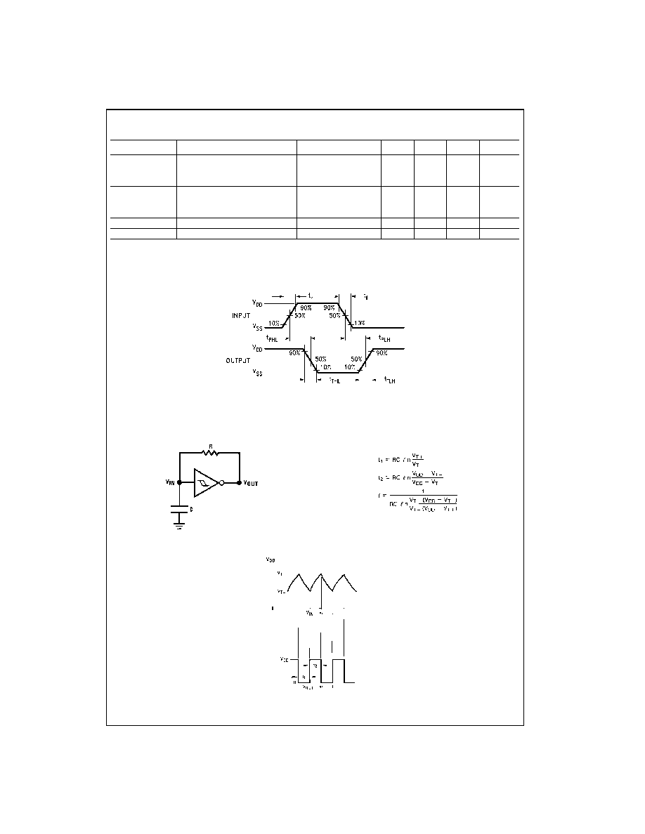
Switching Time Waveforms
t
r
=
t
f
=
20 ns
Typical Applications
Low Power Oscillator
Note: The equations assume
t
1
+
t
2
>>
t
PHL
+
t
PLH
Symbol
Parameter
Conditions
Min
Typ
Max
Units
t
PHL
or t
PLH
Propagation Delay Time from
V
DD
=
5V
220
400
ns
Input to Output
V
DD
=
10V
80
200
ns
V
DD
=
15V
70
160
ns
t
THL
or t
TLH
Transition Time
V
DD
=
5V
100
200
ns
V
DD
=
10V
50
100
ns
V
DD
=
15V
40
80
ns
C
IN
Average Input Capacitance
Any Input
5
7.5
pF
C
PD
Power Dissipation Capacity
Any Gate (Note 5)
14
pF
www.fairchildsemi.com
4
C
D
401
06BC
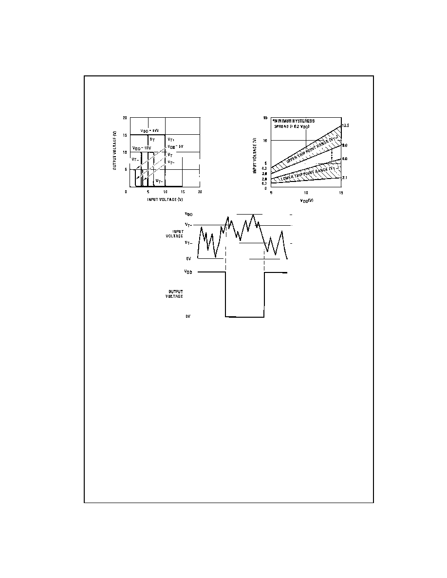
Typical Performance Characteristics
Typical Transfer
Characteristics
Guaranteed
Guaranteed
Trip Point Range
5
www.fairchildsemi.com
CD401
06BC
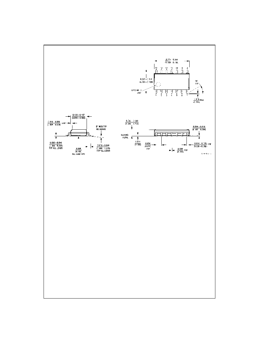
Physical Dimensions
inches (millimeters) unless otherwise noted
16-Lead Small Outline Integrated Circuit (SOIC), JEDEC MS-120, 0.150" Narrow Body
Package Number M14A

Fairchild does not assume any responsibility for use of any circuitry described, no circuit patent licenses are implied and Fairchild reserves the right at any time without notice to change said circuitry and specifications.
CD40106
B
C
He
x Sc
hmit
t T
r
i
g
g
e
r
LIFE SUPPORT POLICY
FAIRCHILD'S PRODUCTS ARE NOT AUTHORIZED FOR USE AS CRITICAL COMPONENTS IN LIFE SUPPORT
DEVICES OR SYSTEMS WITHOUT THE EXPRESS WRITTEN APPROVAL OF THE PRESIDENT OF FAIRCHILD
SEMICONDUCTOR CORPORATION. As used herein:
1. Life support devices or systems are devices or systems
which, (a) are intended for surgical implant into the
body, or (b) support or sustain life, and (c) whose failure
to perform when properly used in accordance with
instructions for use provided in the labeling, can be rea-
sonably expected to result in a significant injury to the
user.
2. A critical component in any component of a life support
device or system whose failure to perform can be rea-
sonably expected to cause the failure of the life support
device or system, or to affect its safety or effectiveness.
www.fairchildsemi.com
Physical Dimensions
inches (millimeters) unless otherwise noted (Continued)
14-Lead Plastic Dual-In-Line Package (PDIP), JEDEC MS-001, 0.300" Wide
Package Number N14A