
October 1987
Revised January 1999
CD401
5BC
Dual
4-
Bit
St
ati
c
Shi
f
t
R
e
gist
er
© 1999 Fairchild Semiconductor Corporation
DS005948.prf
www.fairchildsemi.com
CD4015BC
Dual 4-Bit Static Shift Register
General Description
The CD4015BC contains two identical, 4-stage, serial-
input/parallel-output registers with independent "Data",
"Clock," and "Reset" inputs. The logic level present at the
input of each stage is transferred to the output of that stage
at each positive-going clock transition. A logic high on the
"Reset" input resets all four stages covered by that input.
All inputs are protected from static discharge by a series
resistor and diode clamps to V
DD
and V
SS
.
Features
s
Wide supply voltage range:
3.0V to 18V
s
High noise immunity:
0.45 V
DD
(typ.)
s
Low power TTL:
Fan out of 2 driving 74L
compatibility:
or 1 driving 74LS
s
Medium speed operation:
8 MHz (typ.) clock rate
s
Fully static design:
@V
DD
-
V
SS
=
10V
Applications
∑ Serial-input/parallel-output data queueing
∑ Serial to parallel data conversion
∑ General purpose register
Ordering Code:
Devices also available in Tape and Reel. Specify by appending the suffix letter "X" to the ordering code.
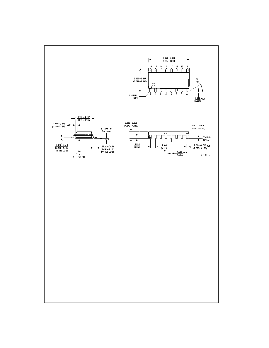
Connection Diagram
Pin Assignments for DIP and SOIC
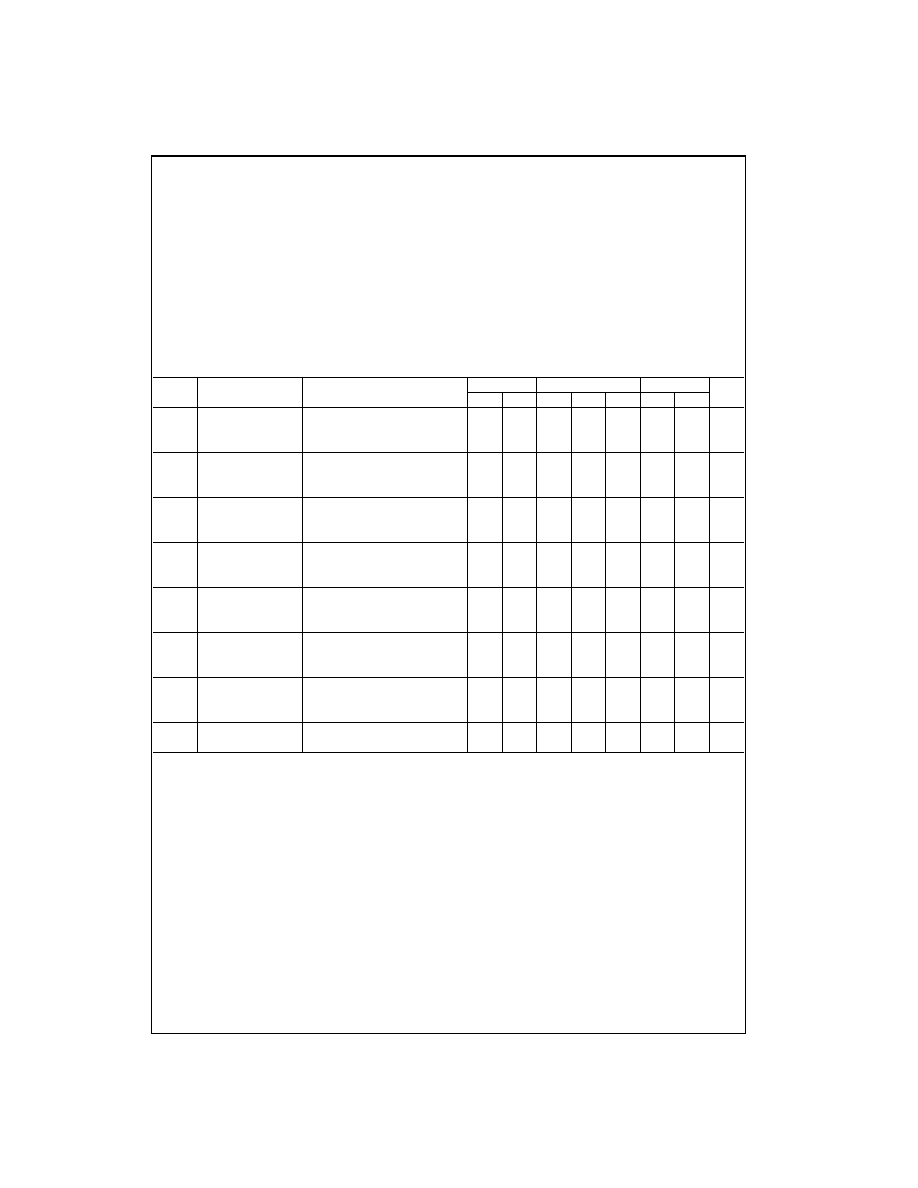
Truth Table
X
=
Don't Care Case
Note 1: Level Change
Order Number
Package Number
Package Description
CD4015BCM
M16A
16-Lead Small Outline Integrated Circuit (SOIC), JEDEC MS-012, 0.150" Narrow
CD4015BCN
N16E
16-Lead Plastic Dual-In-Line Package (PDIP), JEDEC MS-001, 0.300" Wide
CL
(Note 1)
D
R
Q
1
Q
n
0
0
0
Q
n
-
1
1
0
1
Q
n
-
1
X
0
Q
1
Q
n
(No change)
X
X
1
0
0
3
www.fairchildsemi.com
CD401
5BC
Absolute Maximum Ratings
(Note 2)
(Note 3)
Recommended Operating
Conditions
Note 2: "Absolute Maximum Ratings" are those values beyond which the
safety of the device cannot be guaranteed; they are not meant to imply that
the devices should be operated at these limits. The tables of "Recom-
mended Operating Conditions" and "Electrical Characteristics" provide con-
ditions for actual device operation.
Note 3: V
SS
=
0V unless otherwise specified.
DC Electrical Characteristics
(Note 3)
Note 4: I
OH
and I
OL
are tested one output at a time.
DC Supply Voltage (V
DD
)
-
0.5 to
+
18 V
DC
Input Voltage (V
IN
)
-
0.5 to V
DD
+
0.5 V
DC
Storage Temperature Range (T
S
)
-
65
∞
C to
+
150
∞
C
Power Dissipation (P
D
)
Dual-In-Line
700 mW
Small Outline
500 mW
Lead Temperature (T
L
)
(Soldering, 10 seconds)
260
∞
C
DC Supply Voltage (V
DD
)
+
3 to
+
15 V
DC
Input Voltage (V
IN
)
0 to V
DD
V
DC
Operating Temperature Range (T
A
)
-
40
∞
C to
+
85
∞
C
Symbol
Parameter
Conditions
-
40
∞
C
+
25
∞
C
+
85
∞
C
Units
Min
Max
Min
Typ
Max
Min
Max
I
DD
Quiescent Device
V
DD
=
5V, V
IN
=
V
DD
or V
SS
20
0.005
20
150
µ
A
Current
V
DD
=
10V, V
IN
=
V
DD
or V
SS
40
0.010
40
300
µ
A
V
DD
=
15V, V
IN
=
V
DD
or V
SS
80
0.015
80
600
µ
A
V
OL
LOW Level
V
DD
=
5V
0.05
0
0.05
0.05
V
Output Voltage
V
DD
=
10V
0.05
0
0.05
0.05
V
V
DD
=
15V
0.05
0
0.05
0.05
V
V
OH
HIGH Level
V
DD
=
5V
4.95
4.95
5
4.95
V
Output Voltage
V
DD
=
10V
9.95
9.95
10
9.95
V
V
DD
=
15V
14.95
14.95
15
14.95
V
V
IL
LOW Level
V
DD
=
5V, V
O
=
0.5V or 4.5V
1.5
2.25
1.5
1.5
V
Input Voltage
V
DD
=
10V, V
O
=
1.0V or 9.0V
3.0
4.50
3.0
3.0
V
V
DD
=
15V, V
O
=
1.5V or 13.5V
4.0
6.75
4.0
4.0
V
V
IH
HIGH Level
V
DD
=
5V, V
O
=
0.5V or 4.5V
3.5
3.5
2.75
3.5
V
Input Voltage
V
DD
=
10V, V
O
=
1.0V or 9.0V
7.0
7.0
5.50
7.0
V
V
DD
=
15V, V
O
=
1.5V or 13.5V
11.0
11.0
8.25
11.0
V
I
OL
LOW Level Output
V
DD
=
5V, V
O
=
0.4V
0.52
0.44
0.88
0.36
mA
Current (Note 4)
V
DD
=
10V, V
O
=
0.5V
1.3
1.1
2.25
0.9
mA
V
DD
=
15V, V
O
=
1.5V
3.6
3.0
8.8
2.4
mA
I
OH
HIGH Level Output
V
DD
=
5V, V
O
=
4.6V
-
0.52
-
0.44
-
0.88
-
0.36
mA
Current (Note 4)
V
DD
=
10V, V
O
=
9.5V
-
1.3
-
1.1
-
2.25
-
0.9
mA
V
DD
=
15V, V
O
=
13.5V
-
3.6
-
3.0
-
8.8
-
2.4
mA
I
IN
Input Current
V
DD
=
15V, V
IN
=
0V
-
0.3
-
10
-
5
-
0.3
-
1.0
µ
A
V
DD
=
15V, V
IN
=
15V
0.3
10
-
5
0.3
1.0
µ
A

www.fairchildsemi.com
4
C
D
40
15BC
AC Electrical Characteristics
(Note 5)
T
A
=
25
∞
C, C
L
=
50 pF, R
L
=
200k, t
r
=
t
f
=
20 ns, unless otherwise specified
Note 5: AC Parameters are guaranteed by DC correlated testing.
Symbol
Parameter
Conditions
Min
Typ
Max
Units
CLOCK OPERATION
t
PHL
, t
PLH
Propagation Delay Time
V
DD
=
5V
230
350
ns
V
DD
=
10V
80
160
ns
V
DD
=
15V
60
120
ns
t
THL
, t
TLH
Transition Time
V
DD
=
5V
100
200
ns
V
DD
=
10V
50
100
ns
V
DD
=
15V
40
80
ns
t
WL
, t
WM
Minimum Clock
V
DD
=
5V
160
250
ns
Pulse-Width
V
DD
=
10V
60
110
ns
V
DD
=
15V
50
85
ns
t
rCL
, t
fCL
Clock Rise and
V
DD
=
5V
15
µ
s
Fall Time
V
DD
=
10V
15
µ
s
V
DD
=
15V
15
µ
s
t
SU
Minimum Data
V
DD
=
5V
50
100
µ
s
Set-Up Time
V
DD
=
10V
20
40
µ
s
V
DD
=
15V
15
30
µ
s
f
CL
Maximum Clock
V
DD
=
5V
2
3.5
MHz
Frequency
V
DD
=
10V
4.5
8
MHz
V
DD
=
15V
6
11
MHz
C
IN
Input Capacitance
Clock Input
7.5
10
pF
Other Inputs
5
7.5
pF
RESET OPERATION
t
PHL(R)
Propagation Delay Time
V
DD
=
5V
200
400
ns
V
DD
=
10V
100
200
ns
V
DD
=
15V
80
160
ns
t
WH(R)
Minimum Reset
V
DD
=
5V
135
250
ns
Pulse Width
V
DD
=
10V
40
80
ns
V
DD
=
15V
30
60
ns
5
www.fairchildsemi.com
CD401
5BC
Physical Dimensions
inches (millimeters) unless otherwise noted
16-Lead Small Outline Integrated Circuit (SOIC), JEDEC MS-012, 0.150" Narrow
Package Number M16A
