© 1999 Fairchild Semiconductor Corporation
DS005987
www.fairchildsemi.com
October 1987
Revised July 1999
CD401
74BC
∑ C
D
40
175BC
Hex D-T
ype Fli
p
-
F
lop ∑
Quad D-T
ype Fli
p
-
F
lop
CD40174BC ∑ CD40175BC
Hex D-Type Flip-Flop ∑ Quad D-Type Flip-Flop
General Description
The CD40174BC consists of six positive-edge triggered D-
type flip-flops; the true outputs from each flip-flop are exter-
nally available. The CD40175BC consists of four positive-
edge triggered D-type flip-flops; both the true and comple-
ment outputs from each flip-flop are externally available.
All flip-flops are controlled by a common clock and a com-
mon clear. Information at the D inputs meeting the set-up
time requirements is transferred to the Q outputs on the
positive-going edge of the clock pulse. The clearing opera-
tion, enabled by a negative pulse at Clear input, clears all
Q outputs to logical "0" and Q s (CD40175BC only) to logi-
cal "1".
All inputs are protected from static discharge by diode
clamps to V
DD
and V
SS
.
Features
s
Wide supply voltage range:
3V to 15V
s
High noise immunity:
0.45 V
DD
(typ.)
s
Low power TTL compatibility:
fan out of 2 driving 74L or 1 driving 74 LS
s
Equivalent to MC14174B, MC14175B
s
Equivalent to MM74C174, MM74C175
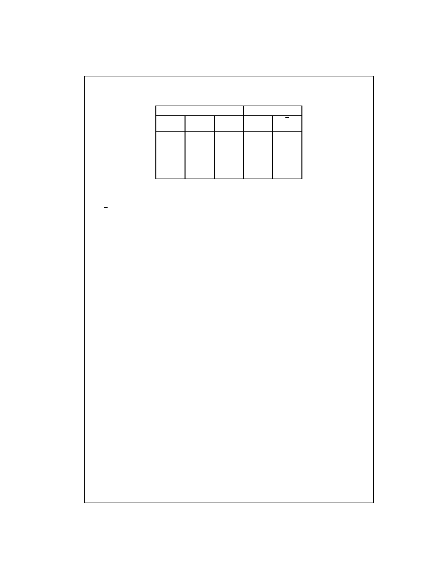
Ordering Code:
Devices also available in Tape and Reel. Specify by appending the suffix letter "X" to the ordering code.
Connection Diagrams
Pin Assignments for DIP and SOIC
CD40174B
Top View
CD40175B
Top View
Order Number
Package Number
Package Description
CD40174BCM
M16A
16-Lead Small Outline Integrated Circuit (SOIC), JEDEC MS-012, 0.150" Narrow Body
CD40174BCN
N16E
16-Lead Plastic Dual-In-Line Package (PDIP), JEDEC MS-001, 0.300" Wide
CD40175BCM
M16A
16-Lead Small Outline Integrated Circuit (SOIC), JEDEC MS-012, 0.150" Narrow Body
CD40175BCN
N16E
16-Lead Plastic Dual-In-Line Package (PDIP), JEDEC MS-001, 0.300" Wide

3
www.fairchildsemi.com
CD401
74BC
∑ C
D
40
175BC
Absolute Maximum Ratings
(Note 2)
(Note 3)
Recommended Operating
Conditions
(Note 3)
Note 2: "Absolute Maximum Ratings" are those values beyond which the
safety of the device cannot be guaranteed. They are not meant to imply
that the devices should be operated at these limits. The tables of "Recom-
mended Operating Conditions" and "Electrical Characteristics" provide con-
ditions for actual device operation.
Note 3: V
SS
=
0V unless otherwise specified.
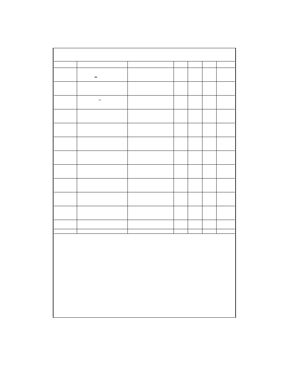
DC Electrical Characteristics
(Note 3)
CD40174BC/CD40175BC
Note 4: I
OH
and I
OL
are tested one output at a time.
DC Supply Voltage (V
DD
)
-
0.5V to
+
18V
Input Voltage (V
IN
)
-
0.5V to V
DD
+
0.5V
DC
Storage Temperature Range (T
S
)
-
65
∞
C to
+
150
∞
C
Power Dissipation (P
D
)
Dual-In-Line
700 mW
Small Outline
500 mW
Lead Temperature (T
L
)
(Soldering, 10 seconds)
260
∞
C
DC Supply Voltage (V
DD
)
3V to 15 V
DC
Input Voltage (V
IN
)
0V to V
DD
V
DC
Operating Temperature Range (T
A
)
-
40
∞
C to
+
85
∞
C
Symbol
Parameter
Conditions
-
40
∞
C
+
25
∞
C
+
85
∞
C
Units
Min
Max
Min
Typ
Max
Min
Max
I
DD
Quiescent Device
V
DD
=
5V, V
IN
=
V
DD
or V
SS
4
4
30
µ
A
Current
V
DD
=
10V, V
IN
=
V
DD
or V
SS
8
8
60
µ
A
V
DD
=
15V, V
IN
=
V
DD
or V
SS
16
16
120
µ
A
V
OL
LOW
Level V
DD
=
5V
0.05
0.05
0.05
V
Output Voltage
V
DD
=
10V
0.05
0.05
0.05
V
V
DD
=
15V
0.05
0.05
0.05
V
V
OH
HIGH Level
V
DD
=
5V
4.95
4.95
5
4.95
V
Output Voltage
V
DD
=
10V
9.95
9.95
10
9.95
V
V
DD
=
15V
14.95
14.95
15
14.95
V
V
IL
LOW
Level V
DD
=
5V, V
O
=
0.5V or 4.5V
1.5
1.5
1.5
V
Input Voltage
V
DD
=
10V, V
O
=
1V or 9V
3.0
3.0
3.0
V
V
DD
=
15V, V
O
=
1.5V or 13.5V
4.0
4.0
4.0
V
V
IH
HIGH Level
V
DD
=
5V, V
O
=
0.5V or 4.5V
3.5
3.5
3.5
V
Input Voltage
V
DD
=
10V, V
O
=
1V or 9V
7.0
7.0
7.0
V
V
DD
=
15V, V
O
=
1.5V or 13.5V
11.0
11.0
11.0
V
I
OL
LOW Level Output
V
DD
=
5V, V
O
=
0.4V
0.52
0.44
0.88
0.36
mA
Current (Note 4)
V
DD
=
10V, V
O
=
0.5V
1.3
1.1
2.25
0.9
mA
V
DD
=
15V, V
O
=
1.5V
3.6
3.0
8.8
2.4
mA
I
OH
HIGH Level Output
V
DD
=
5V, V
O
=
4.6V
-
0.52
-
0.44
-
0.88
-
0.36
mA
Current (Note 4)
V
DD
=
10V, V
O
=
9.5V
-
1.3
-
1.1
-
2.25
-
0.9
mA
V
DD
=
15V, V
O
=
13.5V
-
3.6
-
3.0
-
8.8
-
2.4
mA
I
IN
Input Current
V
DD
=
15V, V
IN
=
0V
-
0.30
-
10
-
5
-
0.30
-
1.0
µ
A
V
DD
=
15V, V
IN
=
15V
0.30
10
-
5
0.30
1.0
µ
A
www.fairchildsemi.com
4
CD4017
4BC
∑ C
D
401
75BC
AC Electrical Characteristics
(Note 5)
T
A
=
25
∞
C, C
L
=
50 pF, R
L
=
200k and t
r
=
t
f
=
20 ns, unless otherwise specified
Note 5: AC Parameters are guaranteed by DC correlated testing.
Note 6: C
PD
determines the no load AC power consumption of any CMOS device. For complete explanation, see 74C Family Characteristics application
note, AN-90.
Symbol
Parameter
Conditions
Min
Typ
Max
Units
t
PHL
, t
PLH
Propagation Delay Time to a
V
DD
=
5V
190
300
ns
Logical "0" or Logical "1" from
V
DD
=
10V
75
110
ns
Clock to Q or Q (CD40175 Only)
V
DD
=
15V
60
90
ns
t
PHL
Propagation Delay Time to a
V
DD
=
5V
180
300
ns
Logical "0" from Clear to Q
V
DD
=
10V
70
110
ns
V
DD
=
15V
60
90
ns
t
PLH
Propagation Delay Time to a Logical
V
DD
=
5V
230
400
ns
"1" from Clear to Q (CD40175 Only)
V
DD
=
10V
90
150
ns
V
DD
=
15V
75
120
ns
t
SU
Time Prior to Clock Pulse that
V
DD
=
5V
45
100
ns
Data must be Present
V
DD
=
10V
15
40
ns
V
DD
=
15V
13
35
ns
t
H
Time after Clock Pulse that
V
DD
=
5V
-
11
0
ns
Data Must be Held
V
DD
=
10V
-
4
0
ns
V
DD
=
15V
-
3
0
ns
t
THL
, t
TLH
Transition Time
V
DD
=
5V
100
200
ns
V
DD
=
10V
50
100
ns
V
DD
=
15V
40
80
ns
t
WH
, t
WL
Minimum Clock Pulse Width
V
DD
=
5V
130
250
ns
V
DD
=
10V
45
100
ns
V
DD
=
15V
40
80
ns
t
WL
Minimum Clear Pulse Width
V
DD
=
5V
120
250
ns
V
DD
=
10V
45
100
ns
V
DD
=
15V
40
80
ns
t
RCL
Maximum Clock Rise Time
V
DD
=
5V
15
µ
s
V
DD
=
10V
5.0
µ
s
V
DD
=
15V
5.0
µ
s
t
fCL
Maximum Clock Fall Time
V
DD
=
5V
15
50
µ
s
V
DD
=
10V
5.0
50
µ
s
V
DD
=
15V
5.0
50
µ
s
f
CL
Maximum Clock Frequency
V
DD
=
5V
2.0
3.5
MHz
V
DD
=
10V
5.0
10
MHz
V
DD
=
15V
6.0
12
MHz
C
IN
Input Capacitance
Clear Input
10
15
pF
Other Input
5.0
7.5
pF
C
PD
Power Dissipation
Per Package (Note 6)
130
pF