September 1995
Revised April 1999
7
4
VH
C1
1
2
Dual
J-
K Fl
i
p
-Fl
ops wi
th
Prese
t
and Cl
ear
© 1999 Fairchild Semiconductor Corporation
DS012123.prf
www.fairchildsemi.com
74VHC112
Dual J-K Flip-Flops with Preset and Clear
General Description
The VHC112 is an advanced high speed CMOS device
fabricated with silicon gate CMOS technology. It achieves
the high-speed operation similar to equivalent Bipolar
Schottky TTL while maintaining the CMOS low power dissi-
pation.
The VHC112 contains two independent, high-speed JK flip-
flops with Direct Set and Clear inputs. Synchronous state
changes are initiated by the falling edge of the clock. Trig-
gering occurs at a voltage level of the clock and is not
directly related to transition time. The J and K inputs can
change when the clock is in either state without affecting
the flip-flop, provided that they are in the desired state dur-
ing the recommended setup and hold times relative to the
falling edge of the clock. The LOW signal on PR or CLR
prevents clocking and forces Q and Q HIGH, respectively.
Simultaneous LOW signals on PR and CLR force both Q
and Q HIGH.
An input protection circuit ensures that 0V to 7V can be
applied to the input pins without regard to the supply volt-
age. This device can be used to interface 5V to 3V systems
and two supply systems such as battery backup. This cir-
cuit prevents device destruction due to mismatched supply
and input voltages.
Features
s
High speed: f
MAX
= 200 MHz (typ) at V
CC
= 5.0V
s
Low power dissipation: I
CC
= 2
µ
A (max) at T
A
= 25
∞
C
s
High noise immunity: V
NIH
= V
NIL
= 28% V
CC
(min)
s
Power down protection is provided on all inputs
s
Pin and function compatible with 74HC112
Ordering Code:
Surface mount packages are also available on Tape and Reel. Specify by appending the suffix letter "X" to the ordering code.
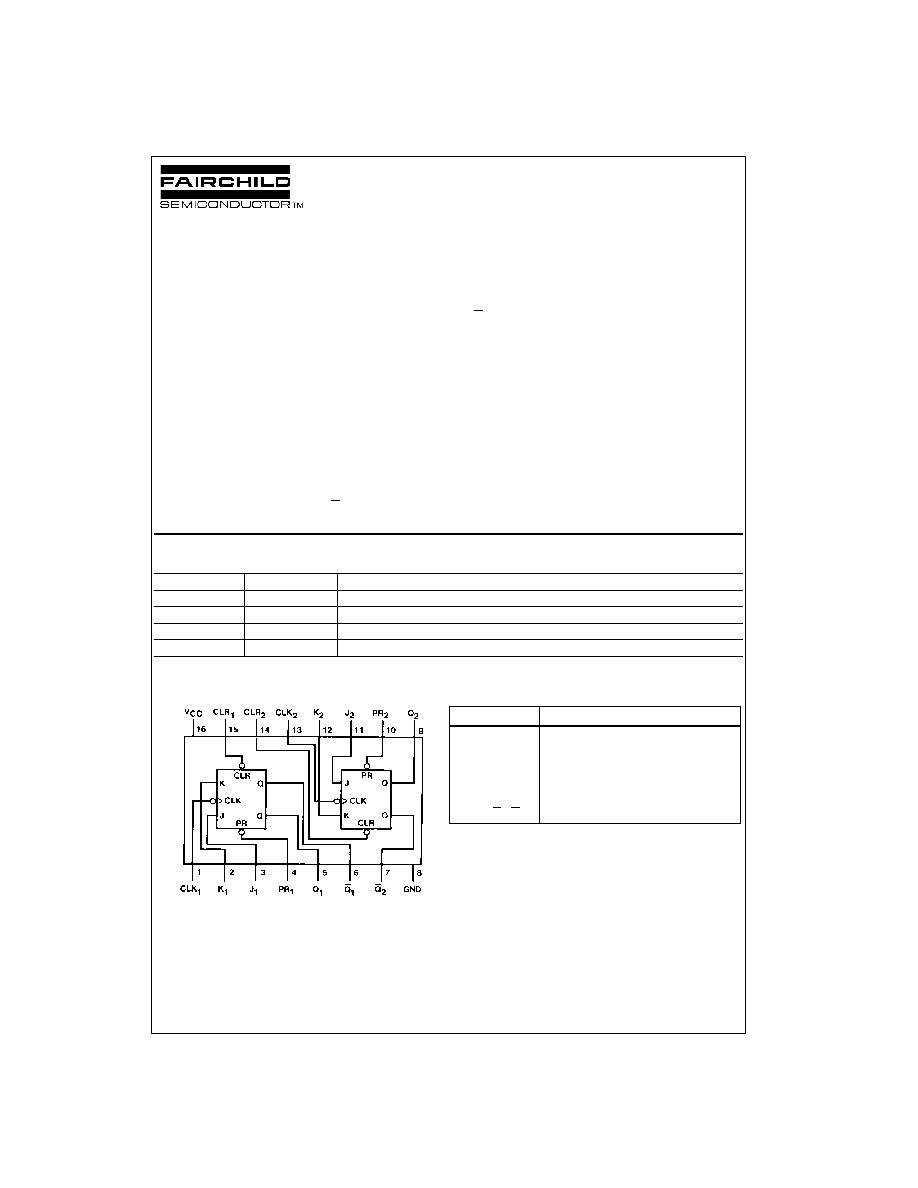
Connection Diagram
Pin Descriptions
Order Number
Package Number
Package Description
74VHC112M
M16A
16-Lead Small Outline Integrated Circuit (SOIC), JEDEC MS-012, 0.150 Narrow
74VHC112SJ
M16D
16-Lead Small Outline Package (SOP), EIAJ TYPE II, 5.3mm Wide
74VHC112MTC
MTC16
16-Lead Thin Shrink Small Outline Package (TSSOP), JEDEC MO-153, 4.4mm Wide
74VHC112N
N16E
16-Lead Plastic Dual-In-Line Package (PDIP), JEDEC MS-001, 0.300 Wide
Pin Names
Description
J
1
, J
2
, K
1
, K
2
Data Inputs
CLK
1
, CLK
2
Clock Pulse Inputs (Active Falling Edge)
CLR
1
, CLR
2
Direct Clear Inputs (Active LOW)
PR
1
, PR
2
Direct Preset Inputs (Active LOW)
Q
1
, Q
2
, Q
1
, Q
2
Outputs

www.fairchildsemi.com
2
74
V
HC1
12
Truth Table
H (h)
=
HIGH Voltage Level
L (l)
=
LOW Voltage Level
X
=
Immaterial
=
HIGH-to-LOW Clock Transition
Q
0
(Q
0
)
=
Before HIGH-to-LOW Transition of Clock
Lower case letters indicate the state of the referenced input or output one setup time prior to the HIGH-to-LOW clock transition.
Logic Diagram
(One Half Shown)
Inputs
Outputs
PR
CLR
CP
J
K
Q
Q
L
H
X
X
X
H
L
H
L
X
X
X
L
H
L
L
X
X
X
H
H
H
H
h
h
Q
0
Q
0
H
H
l
h
L
H
H
H
h
l
H
L
H
H
l
l
Q
0
Q
0

3
www.fairchildsemi.com
7
4
VH
C1
1
2
Absolute Maximum Ratings
(Note 1)
Recommended Operating
Conditions
(Note 2)
Note 1: Absolute Maximum Ratings are values beyond which the device
may be damaged or have its useful life impaired. The databook specifica-
tions should be met, without exception, to ensure that the system design is
reliable over its power supply, temperature, and output/input loading vari-
ables. Fairchild does not recommend operation outside databook specifica-
tions.
Note 2: Unused inputs must be held HIGH or LOW. They may not float.
DC Electrical Characteristics
Supply Voltage (V
CC
)
-
0.5V to
+
7.0V
DC Input Voltage (V
IN
)
-
0.5V to
+
7.0V
DC Output Voltage (V
OUT
)
-
0.5V to V
CC
+
0.5V
Input Diode Current (I
IK
)
-
20 mA
Output Diode Current (I
OK
)
±
20 mA
DC Output Current (I
OUT
)
±
25 mA
DC V
CC
/GND Current (I
CC
)
±
50 mA
Storage Temperature (T
STG
)
-
65
∞
C to
+
150
∞
C
Lead Temperature (T
L
)
(Soldering, 10 seconds)
260
∞
C
Supply Voltage (V
CC
)
2.0V to
+
5.5V
Input Voltage (V
IN
)
0V to
+
5.5V
Output Voltage (V
OUT
)
0V to V
CC
Operating Temperature (T
OPR
)
-
40
∞
C to
+
85
∞
C
Input Rise and Fall Time (t
r
, t
f
)
V
CC
=
3.3V
±
0.3V
0
100 ns/V
V
CC
=
5.0V
±
0.5V
0
20 ns/V
Symbol
Parameter
V
CC
(V)
T
A
=
25
∞
C
T
A
=
-
40
∞
C to
+
85
∞
C
Units
Conditions
Min
Typ
Max
Min
Max
V
IH
HIGH Level
2.0
1.50
1.50
V
Input Voltage
3.0
-
5.5
0.7 V
CC
0.7 V
CC
V
IL
LOW Level
2.0
0.50
0.50
V
Input Voltage
3.0
-
5.5
0.3 V
CC
0.3 V
CC
V
OH
HIGH Level
2.0
1.9
2.0
1.9
V
IN
=
V
IH
I
OH
=
-
50
µ
A
Output Voltage
3.0
2.9
3.0
2.9
V
or V
IL
4.5
4.4
4.5
4.4
3.0
2.58
2.48
V
I
OH
=
-
4 mA
4.5
3.94
3.80
I
OH
=
-
8 mA
V
OL
LOW Level
2.0
0.0
0.1
0.1
V
IN
=
V
IH
I
OL
=
50
µ
A
Output Voltage
3.0
0.0
0.1
0.1
V
or V
IL
4.5
0.0
0.1
0.1
3.0
0.36
0.44
V
I
OL
=
4 mA
4.5
0.36
0.44
I
OL
=
8 mA
I
IN
Input Leakage Current
0
-
5.5
±
0.1
±
1.0
µ
A
V
IN
=
5.5V or GND
I
CC
Quiescent Supply Current
5.5
2.0
20.0
µ
A
V
IN
=
V
CC
or GND

www.fairchildsemi.com
4
74
V
HC1
12
AC Electrical Characteristics
Note 3: C
PD
is defined as the value of the internal equivalent capacitance which is calculated from the operating current consumption without load. Average
operating current can be obtained from the equation: I
CC
(opr.)
=
C
PD
* V
CC
* f
IN
+
I
CC
/4 (per F/F), and the total C
PD
when n pcs of the Flip-Flop operate can
be calculated by the following equation: C
PD
(total)
=
30
+
14 ∑ n
AC Operating Requirements
Note 4: V
CC
is 3.3
±
0.3V or 5.0
±
0.5V
Symbol
Parameter
V
CC
(V)
T
A
=
25
∞
C
T
A
=
-
40
∞
C to
+
85
∞
C
Units
Conditions
Min
Typ
Max
Min
Max
f
MAX
Maximum Clock
3.3
±
0.3
110
150
100
MHz
C
L
=
15 pF
Frequency
90
120
80
C
L
=
50 pF
5.0
±
0.5
150
200
135
MHz
C
L
=
15 pF
120
185
110
C
L
=
50 pF
t
PLH
Propagation Delay
3.3
±
0.3
8.5
11.0
1.0
13.4
ns
C
L
=
15 pF
t
PHL
Time (CP to Q
n
or Q
n
)
10.0
15.0
1.0
16.5
C
L
=
50 pF
5.0
±
0.5
5.1
7.3
1.0
8.8
ns
C
L
=
15 pF
6.3
10.5
1.0
12.0
C
L
=
50 pF
t
PLH
Propagation Delay Time
3.3
±
0.3
6.7
10.2
1.0
11.7
ns
C
L
=
15 pF
t
PHL
(PR or CLR to Q
n
or Q
n
)
9.7
13.5
1.0
15.0
C
L
=
50 pF
5.0
±
0.5
4.6
6.7
1.0
8.0
ns
C
L
=
15 pF
6.4
9.5
1.0
11.0
C
L
=
50 pF
C
IN
Input Capacitance
4
10
10
pF
V
CC
=
Open
C
PD
Power Dissipation
18
pF
(Note 3)
Capacitance
Symbol
Parameter
V
CC
(Note 4)
(V)
T
A
=
25
∞
C
T
A
=
-
40
∞
C to
+
85
∞
C
Units
Typ
Guaranteed Minimum
t
W
Minimum Pulse Width
3.3
5.0
5.0
ns
(CP or CLR or PR)
5.0
5.0
5.0
t
S
Minimum Setup Time
3.3
5.0
5.0
ns
(J
n
or K
n
to CP
n
)
5.0
4.0
4.0
t
H
Minimum Hold Time
3.3
1.0
1.0
ns
(J
n
or K
n
to CP
n
)
5.0
1.0
1.0
t
REC
Minimum Recovery Time
3.3
6.0
6.0
ns
(CLR or PR to CP)
5.0
5.0
5.0

5
www.fairchildsemi.com
7
4
VH
C1
1
2
Physical Dimensions
inches (millimeters) unless otherwise noted
16-Lead Small Outline Integrated Circuit (SOIC), JEDEC MS-012, 0.150 Narrow
Package Number M16A
16-Lead Small Outline Package (SOP), EIAJ TYPE II, 5.3mm Wide
Package Number M16D