October 1987
Revised January 1999
CD404
3BC
·
CD404
4BC
Quad
3
-
ST
A
T
E
NOR
R/
S
Lat
c
hes ·
Quad 3-ST
A
T
E
NAND
R/
S
Lat
c
hes
© 1999 Fairchild Semiconductor Corporation
DS005967.prf
www.fairchildsemi.com
CD4043BC · CD4044BC
Quad 3-STATE NOR R/S Latches ·
Quad 3-STATE NAND R/S Latches
General Description
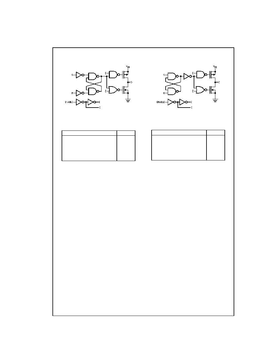
The CD4043BC are quad cross-couple 3-STATE CMOS
NOR latches, and the CD4044BC are quad cross-couple 3-
STATE CMOS NAND latches. Each latch has a separate Q
output and individual SET and RESET inputs. There is a
common 3-STATE ENABLE input for all four latches. A
logic "1" on the ENABLE input connects the latch states to
the Q outputs. A logic "0" on the ENABLE input discon-
nects the latch states from the Q outputs resulting in an
open circuit condition on the Q output. The 3-STATE fea-
ture allows common bussing of the outputs.
Features
s
Wide supply voltage range:
3V to 15V
s
Low power:
100 nW (typ.)
s
High noise immunity:
0.45 V
DD
(typ.)
s
Separate SET and RESET inputs for each latch
s
NOR and NAND configuration
s
3-STATE output with common output enable
Applications
· Multiple bus storage
· Strobed register
· Four bits of independent storage with output enable
· General digital logic
Ordering Code:
Devices also available in Tape and Reel. Specify by appending the suffix letter "X" to the ordering code.
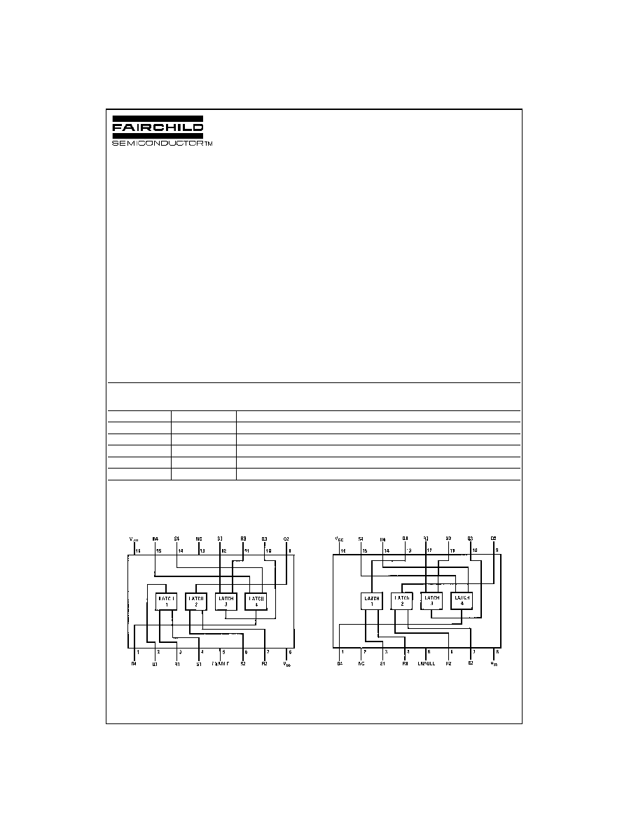
Connection Diagrams
Pin Assignments for DIP, SOIC and SOP
CD4043BC
Top View
Pin Assignments for DIP and SOIC
CD4044BC
Top View
Order Number
Package Number
Package Description
CD4043BCM
M16A
16-Lead Small Outline Integrated Circuit (SOIC), JEDEC MS-012, 0.150" Narrow Body
CD4043BCN
N16E
16-Lead Plastic Dual-In-Line Package (PDIP), JEDEC MS-001, 0.300" Wide
CD4044BCM
M16A
16-Lead Small Outline Integrated Circuit (SOIC), JEDEC MS-012, 0.150" Narrow Body
CD4044BCSJ
M16D
16-Lead Small Outline Package (SOP), EIAJ TYPE II, 5.3mm Wide
CD4044BCN
N16E
16-Lead Plastic Dual-In-Line Package (PDIP), JEDEC MS-001, 0.300" Wide
3
www.fairchildsemi.com
CD404
3BC
· CD404
4BC
Absolute Maximum Ratings
(Note 1)
(Note 2)
Recommended Operating
Conditions
(Note 2)
Note 1: "Absolute Maximum Ratings" are those values beyond which the
safety of the device cannot be guaranteed; they are not meant to imply that
the devices should be operated at these limits. The tables of "Recom-
mended Operating Conditions" and "Electrical Characteristics" provide con-
ditions for actual device operation.
Note 2: V
SS
=
0V unless otherwise specified.
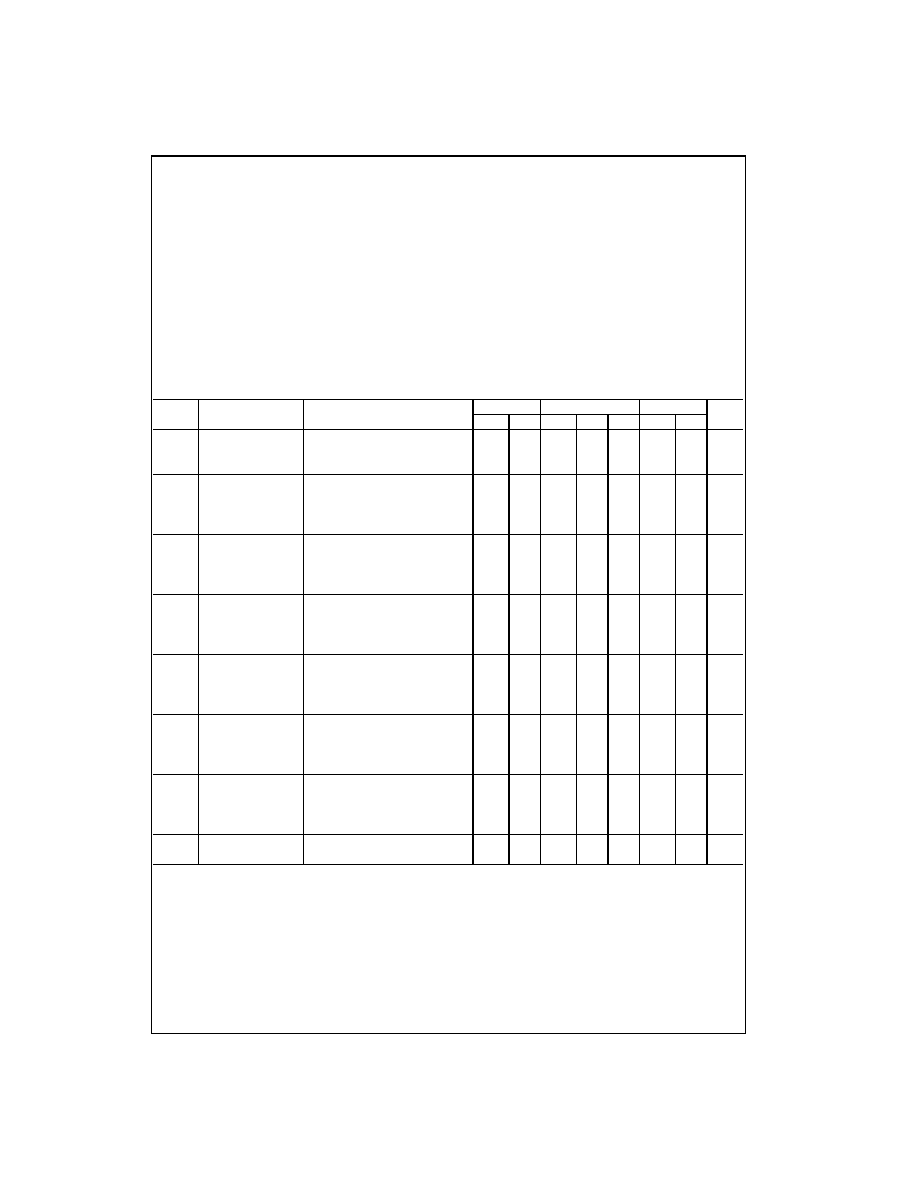
DC Electrical Characteristics
(Note 2)
Note 3: I
OH
and I
OL
are tested one output at a time.
Supply Voltage (V
DD
)
-
0.5V to
+
18V
Input Voltage (V
IN
)
-
0.5V to V
DD
+
0.5V
Storage Temperature Range (T
S
)
-
65
°
C to
+
150
°
C
Power Dissipation (P
D
)
Dual-In-Line
700 mW
Small Outline
500 mW
Lead Temperature (T
L
)
(Soldering, 10 seconds)
260
°
C
Supply Voltage (V
DD
)
3.0V to 15V
Input Voltage (V
IN
)
0 to V
DD
V
Operating Temperature Range (T
A
)
CD4043BC, CD4044BC
-
40
°
C to
+
85
°
C
Symbol
Parameter
Conditions
-
40
°
C
+
25
°
C
+
85
°
C
Units
Min
Max
Min
Typ
Max
Min
Max
I
DD
Quiescent
V
DD
=
5V, V
IN
=
V
DD
or V
SS
20
0.01
20
150
µ
A
Device Current
V
DD
=
10V, V
IN
=
V
DD
or V
SS
40
0.01
40
300
µ
A
V
DD
=
15V, V
IN
=
V
DD
or V
SS
80
0.02
80
600
µ
A
V
OL
LOW Level
|I
O
|
1
µ
A, V
IL
=
0V, V
IH
=
V
DD
Output Voltage
V
DD
=
5.0V
0.05
0
0.05
0.05
V
V
DD
=
10V
0.05
0
0.05
0.05
V
V
DD
=
15V
0.05
0
0.05
0.05
V
V
OH
HIGH Level
|I
O
|
1
µ
A, V
IL
=
0V, V
IH
=
V
DD
Output Voltage
V
DD
=
5.0V
4.95
4.95
5.0
4.95
V
V
DD
=
10V
9.95
9.95
10
9.95
V
V
DD
=
15V
14.95
14.95
15
14.95
V
V
IL
LOW Level
|I
O
|
1
µ
A
Input Voltage
V
DD
=
5.0V, V
O
=
0.5V or 4.5V
1.5
2.25
1.5
1.5
V
V
DD
=
10V, V
O
=
1.0V or 9.0V
3.0
4.5
3.0
3.0
V
V
DD
=
15V, V
O
=
1.5V or 13.5V
4.0
6.75
4.0
4.0
V
V
IH
HIGH Level
|I
O
|
1
µ
A
Input Voltage
V
DD
=
5.0V, V
O
=
0.5V or 4.5V
3.5
3.5
3.5
V
V
DD
=
5.0V, V
O
=
1.0V or 9.0V
7.0
7.0
7.0
V
V
DD
=
15V, V
O
=
1.5V or 13.5V
11
11
11
V
I
OL
LOW Level
V
IL
=
0V, V
IH
=
V
DD
Output Current
V
DD
=
5.0V, V
O
=
0.4V
0.52
0.44
0.88
0.36
mA
(Note 3)
V
DD
=
10V, V
O
=
0.5V
1.3
1.1
2.2
0.9
mA
V
DD
=
15V, V
O
=
1.5V
3.6
3.0
6.0
2.4
mA
I
OH
HIGH Level
V
IL
=
0V, V
IH
=
V
DD
Output Current
V
DD
=
5.0V, V
O
=
4.6V
-
0.52
-
0.44
-
0.32
-
0.36
mA
(Note 3)
V
DD
=
10V, V
O
=
9.5V
-
1.3
-
1.1
-
0.8
-
0.9
mA
V
DD
=
15V, V
O
=
13.5V
-
3.6
-
3.0
-
2.4
-
2.4
mA
I
IN
Input Current
V
DD
=
15V, V
IN
=
0V
-
0.3
-
0.3
-
1.0
µ
A
V
DD
=
15V, V
IN
=
15V
0.3
0.3
1.0
µ
A
www.fairchildsemi.com
4
C
D
40
43BC
· C
D
40
44BC
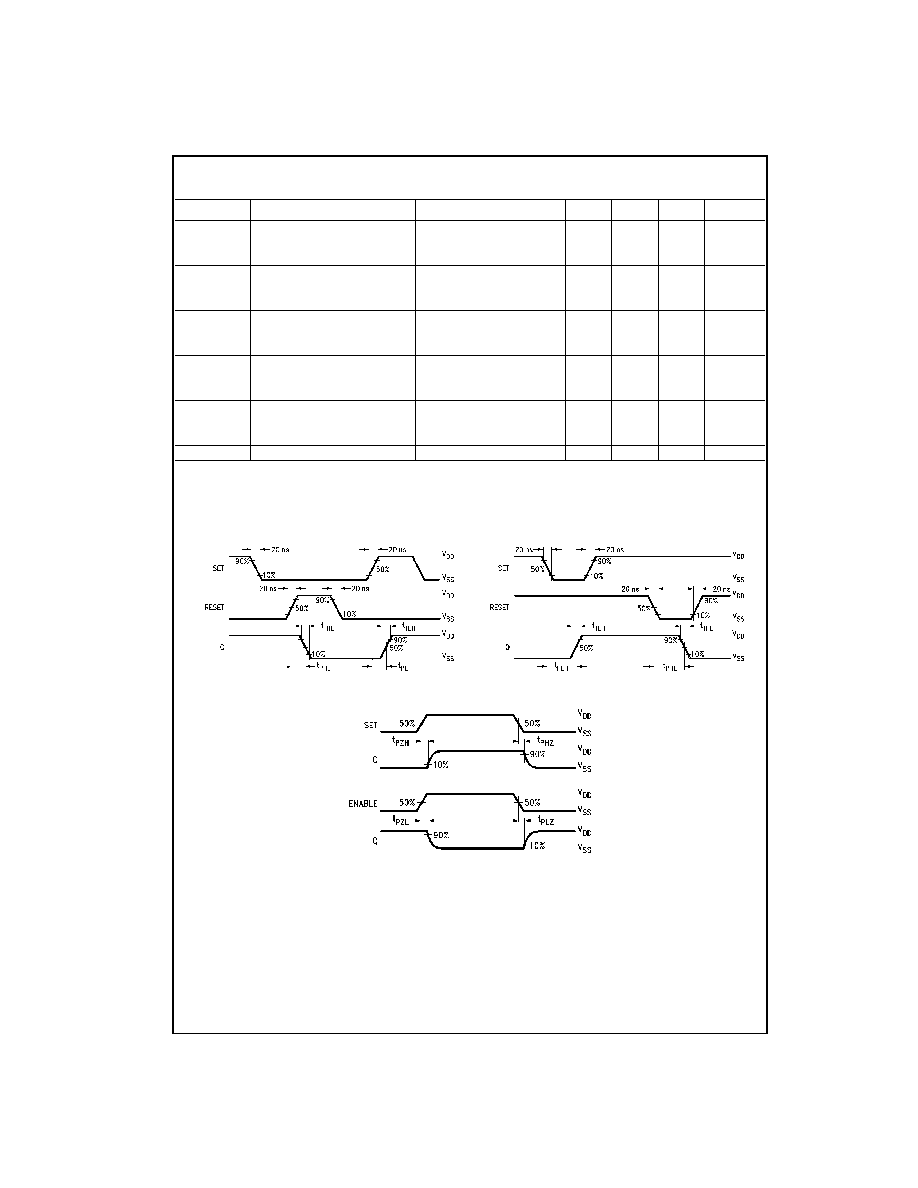
AC Electrical Characteristics
(Note 4)
T
A
=
25
°
C, C
L
=
50 pF, R
L
=
200k, input t
r
=
t
f
=
20 ns, unless otherwise noted
Note 4: AC Parameters are guaranteed by DC correlated testing.
Timing Waveforms
CD4043B
CD4044B
Enable Timing
Symbol
Parameter
Conditions
Min
Typ
Max
Units
t
PLH
, t
PHL
Propagation Delay S or R to Q
V
DD
=
5.0V
175
350
ns
V
DD
=
10V
75
175
ns
V
DD
=
15V
60
120
ns
t
PZH
, t
PHZ
Propagation Delay Enable to Q (HIGH)
V
DD
=
5.0V
115
230
ns
V
DD
=
10V
55
110
ns
V
DD
=
15V
40
80
ns
t
PZL
, t
PLZ
Propagation Delay Enable to Q (LOW)
V
DD
=
5.0V
100
200
ns
V
DD
=
10V
50
100
ns
V
DD
=
15V
40
80
ns
t
THL
, t
TLH
Transition Time
V
DD
=
5.0V
100
200
ns
V
DD
=
10V
50
100
ns
V
DD
=
15V
40
80
ns
t
WO
Minimum SET or RESET Pulse Width
V
DD
=
5.0V
80
160
ns
V
DD
=
10V
40
80
ns
V
DD
=
15V
20
40
ns
C
IN
Input Capacitance
5.0
7.5
pF
5
www.fairchildsemi.com
CD404
3BC
· CD404
4BC
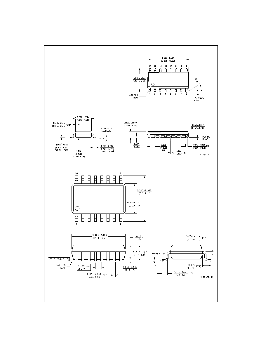
Physical Dimensions
inches (millimeters) unless otherwise noted
16-Lead Small Outline Integrated Circuit (SOIC), JEDEC MS-012, 0.150" Narrow Body
Package Number M16A
16-Lead Small Outline Package (SOP), EIAJ TYPE II, 5.3mm Wide
Package Number M16D