© 2002 Fairchild Semiconductor Corporation
DS005968
www.fairchildsemi.com
October 1987
Revised March 2002
CD404
6BC
Micr
opower Phase-L
o
cked
L
oop
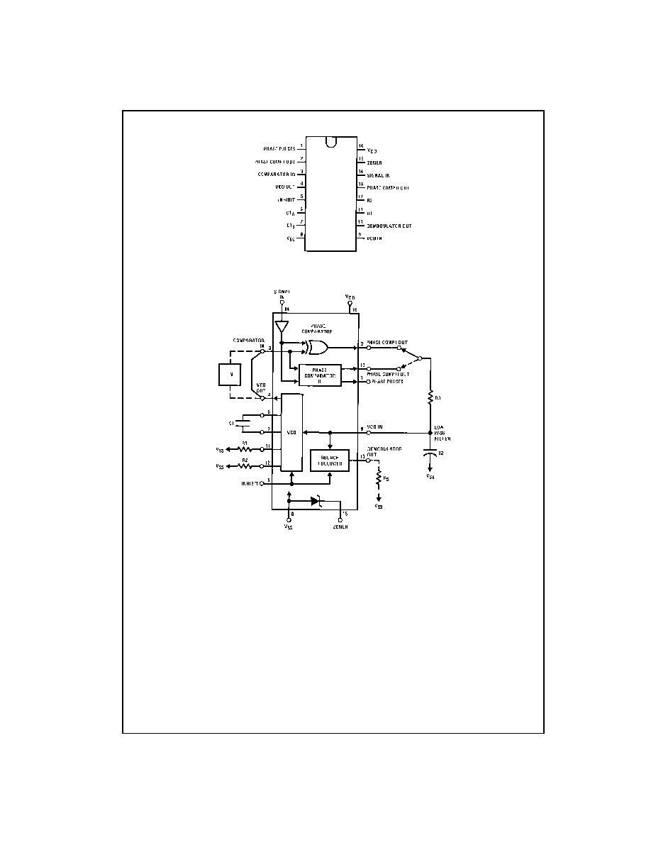
CD4046BC
Micropower Phase-Locked Loop
General Description
The CD4046BC micropower phase-locked loop (PLL) con-
sists of a low power, linear, voltage-controlled oscillator
(VCO), a source follower, a zener diode, and two phase
comparators. The two phase comparators have a common
signal input and a common comparator input. The signal
input can be directly coupled for a large voltage signal, or
capacitively coupled to the self-biasing amplifier at the sig-
nal input for a small voltage signal.
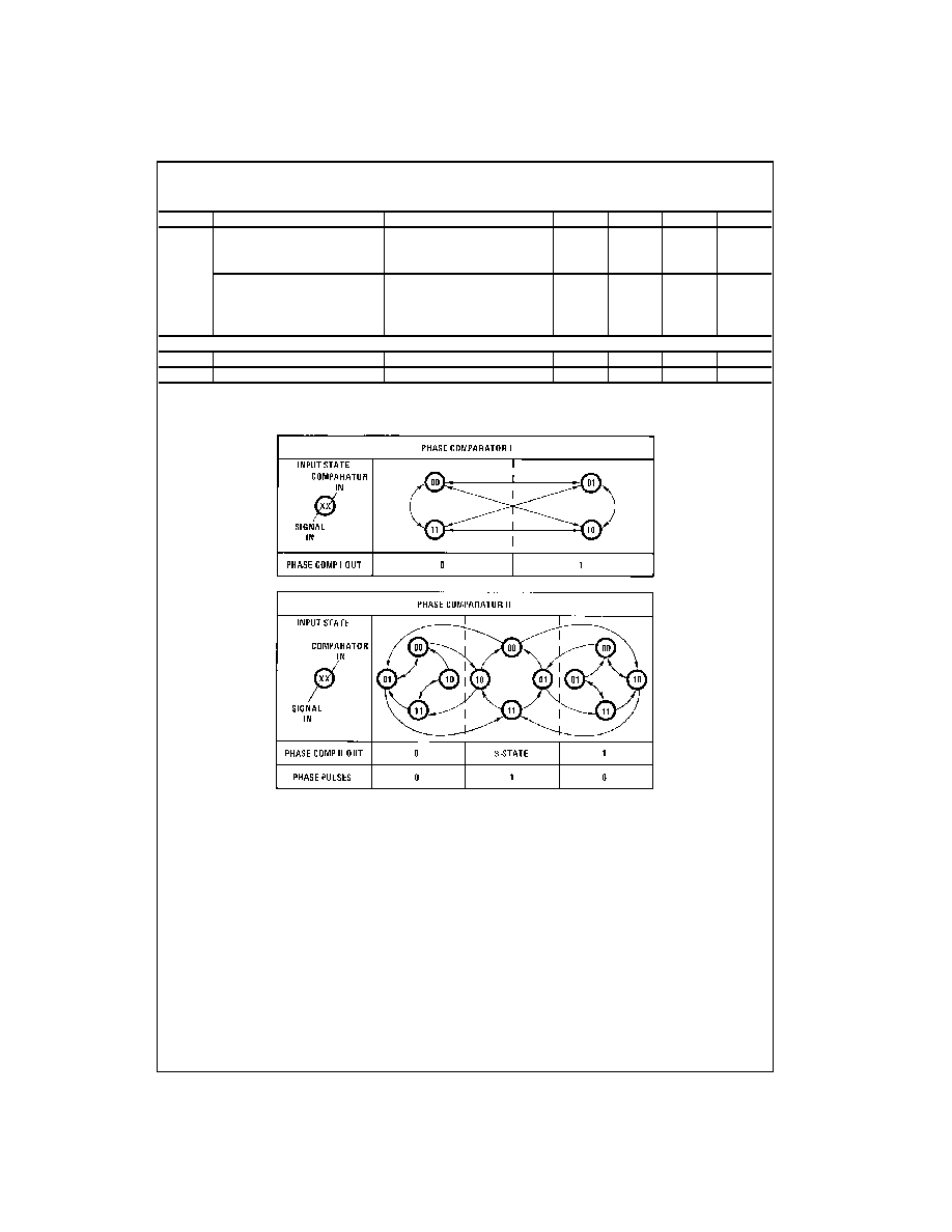
Phase comparator I, an exclusive OR gate, provides a digi-
tal error signal (phase comp. I Out) and maintains 90
°
phase shifts at the VCO center frequency. Between signal
input and comparator input (both at 50% duty cycle), it may
lock onto the signal input frequencies that are close to har-
monics of the VCO center frequency.
Phase comparator II is an edge-controlled digital memory
network. It provides a digital error signal (phase comp. II
Out) and lock-in signal (phase pulses) to indicate a locked
condition and maintains a 0
°
phase shift between signal
input and comparator input.
The linear voltage-controlled oscillator (VCO) produces an
output signal (VCO Out) whose frequency is determined by
the voltage at the VCO
IN
input, and the capacitor and resis-
tors connected to pin C1
A
, C1
B
, R1 and R2.
The source follower output of the VCO
IN
(demodulator Out)
is used with an external resistor of 10 k
or more.
The INHIBIT input, when high, disables the VCO and
source follower to minimize standby power consumption.
The zener diode is provided for power supply regulation, if
necessary.
Features
s
Wide supply voltage range:
3.0V to 18V
s
Low dynamic power consumption:
70
µ
W (typ.)
at f
o
=
10 kHz, V
DD
=
5V
s
VCO frequency:
1.3 MHz (typ.) at V
DD
=
10V
s
Low frequency drift:
0.06%/
°
C at V
DD
=
10V with
temperature
s
High VCO linearity:
1% (typ.)
Applications
· FM demodulator and modulator
· Frequency synthesis and multiplication
· Frequency discrimination
· Data synchronization and conditioning
· Voltage-to-frequency conversion
· Tone decoding
· FSK modulation
· Motor speed control
Ordering Code:
Devices also available in Tape and Reel. Specify by appending the suffix letter "X" to the ordering code.
Order Number
Package Number
Package Description
CD4046BCM
M16A
16-Lead Small Outline Integrated Circuit (SOIC), JEDEC MS-012, 0.150" Narrow
CD4046BCN
N16E
16-Lead Plastic Dual-In-Line Package (PDIP), JEDEC MS-001, 0.300" Wide
3
www.fairchildsemi.com
CD404
6BC
Absolute Maximum Ratings
(Note 1)
(Note 2)
Recommended Operating
Conditions
(Note 2)
Note 1: "Absolute Maximum Ratings" are those values beyond which the
safety of the device cannot be guaranteed. They are not meant to imply
that the devices should be operated at these limits. The table of "Recom-
mended Operating Conditions" and "Electrical Characteristics" provides
conditions for actual device operation.
Note 2: V
SS
=
0V unless otherwise specified.
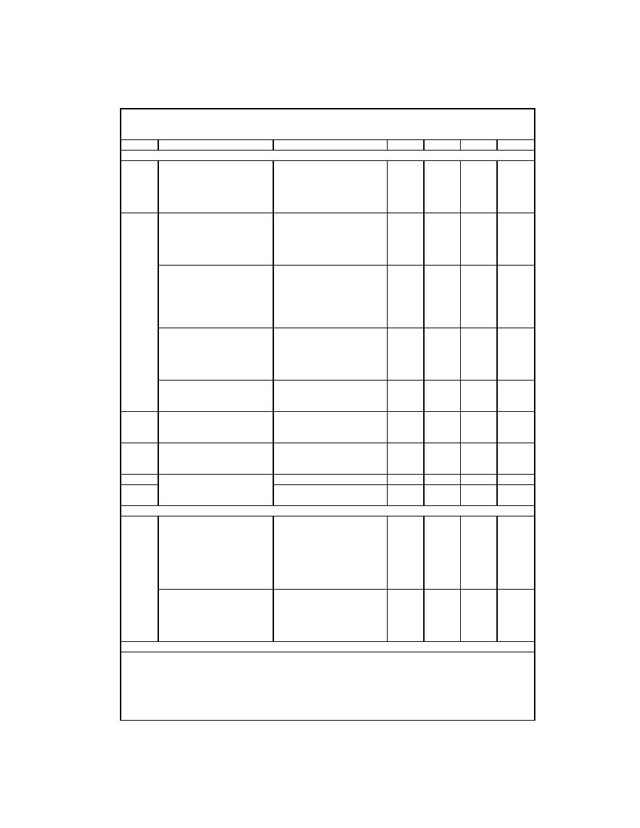
DC Electrical Characteristics
(Note 2)
Note 3: Capacitance is guaranteed by periodic testing.
Note 4: I
OH
and I
OL
are tested one output at a time.
DC Supply Voltage (V
DD
)
-
0.5 to
+
18 V
DC
Input Voltage (V
IN
)
-
0.5 to V
DD
+
0.5 V
DC
Storage Temperature Range (T
S
)
-
65
°
C to
+
150
°
C
Power Dissipation (P
D
)
Dual-In-Line
700 mW
Small Outline
500 mW
Lead Temperature (T
L
)
(Soldering, 10 seconds)
260
°
C
DC Supply Voltage (V
DD
)
3 to 15 V
DC
Input Voltage (V
IN
)
0 to V
DD
V
DC
Operating Temperature Range (T
A
)
-
55
°
C to
+
125
°
C
Symbol
Parameter
Conditions
-
55
°
C
+
25
°
C
+
125
°
C
Units
Min
Max
Min
Typ
Max
Min
Max
I
DD
Quiescent Device Current
Pin 5
=
V
DD,
Pin 14
=
V
DD,
Pin 3, 9
=
V
SS
V
DD
=
5V
5
0.005
5
150
µ
A
V
DD
=
10V
10
0.01
10
300
V
DD
=
15V
20
0.015
20
600
Pin 5
=
V
DD
, Pin 14
=
Open,
Pin 3, 9
=
V
SS
V
DD
=
5V
45
5
35
185
µ
A
V
DD
=
10V
450
20
350
650
V
DD
=
15V
1200
50
900
1500
V
OL
LOW Level Output Voltage
V
DD
=
5V
0.05
0
0.05
0.05
V
V
DD
=
10V
0.05
0
0.05
0.05
V
DD
=
15V
0.05
0
0.05
0.05
V
OH
HIGH Level Output Voltage
V
DD
=
5V
4.95
4.95
5
4.95
V
V
DD
=
10V
9.95
9.95
10
9.95
V
DD
=
15V
14.95
14.95
15
14.95
V
IL
LOW Level Input Voltage
V
DD
=
5V, V
O
=
0.5V or 4.5V
1.5
2.25
1.5
1.5
V
Comparator and Signal In
V
DD
=
10V, V
O
=
1V or 9V
3.0
4.5
3.0
3.0
V
DD
=
15V, V
O
=
1.5V or 13.5V
4.0
6.25
4.0
4.0
V
IH
HIGH Level Input Voltage
V
DD
=
5V, V
O
=
0.5V or 4.5V
3.5
3.5
2.75
3.5
V
Comparator and Signal In
V
DD
=
10V, V
O
=
1V or 9V
7.0
7.0
5.5
7.0
V
DD
=
15V, V
O
=
1.5V or 13.5V
11.0
11.0
8.25
11.0
I
OL
LOW Level Output Current
V
DD
=
5V, V
O
=
0.4V
0.64
0.51
0.88
0.36
mA
(Note 4)
V
DD
=
10V, V
O
=
0.5V
1.6
1.3
2.25
0.9
V
DD
=
15V, V
O
=
1.5V
4.2
3.4
8.8
2.4
I
OH
HIGH Level Output Current
V
DD
=
5V, V
O
=
4.6V
-
0.64
-
0.51
-
0.88
-
0.36
mA
(Note 4)
V
DD
=
10V, V
O
=
9.5V
-
1.6
-
1.3
-
2.25
-
0.9
V
DD
=
15V, V
O
=
13.5V
-
4.2
-
3.4
-
8.8
-
2.4
I
IN
Input Current
All Inputs Except Signal Input
V
DD
=
15V, V
IN
=
0V
-
0.1
-
10
-
5
-
0.1
-
1.0
µ
A
V
DD
=
15V, V
IN
=
15V
0.1
10
-
5
0.1
1.0
C
IN
Input Capacitance
Any Input (Note 3)
7.5
pF
P
T
Total Power Dissipation
f
o
=
10 kHz, R1
=
1 M
,
R2
=
,
VCO
IN
=
V
CC
/2
V
DD
=
5V
0.07
mW
V
DD
=
10V
0.6
V
DD
=
15V
2.4
www.fairchildsemi.com
4
C
D
40
46BC
AC Electrical Characteristics
(Note 5)
T
A
=
25
°
C, C
L
=
50 pF
Symbol
Parameter
Conditions
Min
Typ
Max
Units
VCO SECTION
I
DD
Operating Current
f
o
=
10 kHz, R1
=
1 M
,
R2
=
,
VCO
IN
=
V
CC
/2
V
DD
=
5V
20
µ
A
V
DD
=
10V
90
V
DD
=
15V
200
f
MAX
Maximum Operating Frequency
C1
=
50 pF, R1
=
10 k
,
R2
=
,
VCO
IN
=
V
DD
V
DD
=
5V
0.4
0.8
MHz
V
DD
=
10V
0.6
1.2
V
DD
=
15V
1.0
1.6
Linearity
VCO
IN
=
2.5V
±
0.3V,
%
R1
10 k
, V
DD
=
5V
1
VCO
IN
=
5V
±
2.5V,
R1
400 k
, V
DD
=
10V
1
VCO
IN
=
7.5V
±
5V,
R1
1 M
, V
DD
=
15V
1
Temperature-Frequency Stability
%/
°
C
<
5c1/f. V
DD
No Frequency Offset, f
MIN
=
0
R2
=
V
DD
=
5V
0.120.24
%/
°
C
V
DD
=
10V
0.040.08
V
DD
=
15V
0.0150.03
Frequency Offset, f
MIN
0
V
DD
=
5V
0.060.12
%/
°
C
V
DD
=
10V
0.050.1
V
DD
=
15V
0.030.06
VCO
IN
Input Resistance
V
DD
=
5V
10
6
M
V
DD
=
10V
10
6
V
DD
=
15V
10
6
VCO
Output Duty Cycle
V
DD
=
5V
50
%
V
DD
=
10V
50
V
DD
=
15V
50
t
THL
VCO Output Transition Time
V
DD
=
5V
90
200
ns
t
THL
V
DD
=
10V
50
100
ns
V
DD
=
15V
45
80
PHASE COMPARATORS SECTION
R
IN
Input Resistance
Signal Input
V
DD
=
5V
1
3
M
V
DD
=
10V
0.2
0.7
V
DD
=
15V
0.1
0.3
Comparator Input
V
DD
=
5V
10
6
V
DD
=
10V
10
6
V
DD
=
15V
10
6
AC-Coupled Signal Input Voltage
Sensitivity
C
SERIES
=
1000 pF
f
=
50 kHz
V
DD
=
5V
200
400
mV
V
DD
=
10V
400
800
V
DD
=
15V
700
1400
DEMODULATOR OUTPUT