 | ÐлекÑÑоннÑй компоненÑ: CD4046BCN | СкаÑаÑÑ:  PDF PDF  ZIP ZIP |
Äîêóìåíòàöèÿ è îïèñàíèÿ www.docs.chipfind.ru
October 1987
Revised January 1999
CD404
6BC
Micr
opo
wer Phase-
Loc
ked Loop
© 1999 Fairchild Semiconductor Corporation
DS005968.prf
www.fairchildsemi.com
CD4046BC
Micropower Phase-Locked Loop
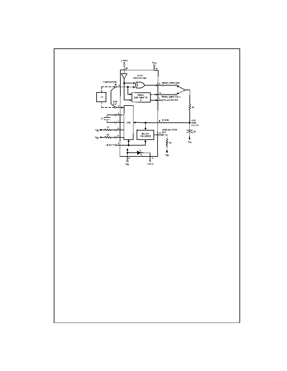
General Description
The CD4046BC micropower phase-locked loop (PLL) con-
sists of a low power, linear, voltage-controlled oscillator
(VCO), a source follower, a zener diode, and two phase
comparators. The two phase comparators have a common
signal input and a common comparator input. The signal
input can be directly coupled for a large voltage signal, or
capacitively coupled to the self-biasing amplifier at the sig-
nal input for a small voltage signal.
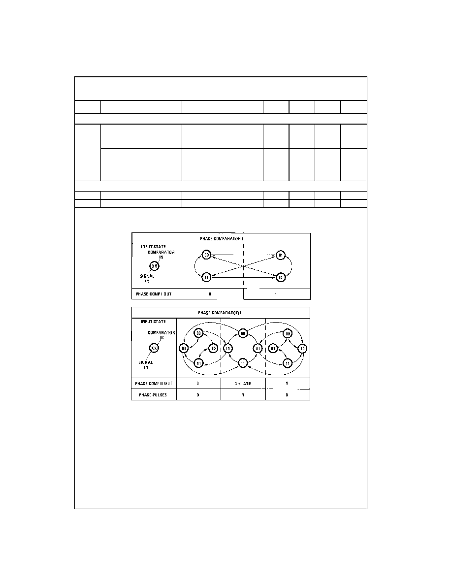
Phase comparator I, an exclusive OR gate, provides a digi-
tal error signal (phase comp. I Out) and maintains 90
°
phase shifts at the VCO center frequency. Between signal
input and comparator input (both at 50% duty cycle), it may
lock onto the signal input frequencies that are close to har-
monics of the VCO center frequency.
Phase comparator II is an edge-controlled digital memory
network. It provides a digital error signal (phase comp. II
Out) and lock-in signal (phase pulses) to indicate a locked
condition and maintains a 0
°
phase shift between signal
input and comparator input.
The linear voltage-controlled oscillator (VCO) produces an
output signal (VCO Out) whose frequency is determined by
the voltage at the VCO
IN
input, and the capacitor and resis-
tors connected to pin C1
A
, C1
B
, R1 and R2.
The source follower output of the VCO
IN
(demodulator Out)
is used with an external resistor of 10 k
or more.
The INHIBIT input, when high, disables the VCO and
source follower to minimize standby power consumption.
The zener diode is provided for power supply regulation, if
necessary.
Features
s
Wide supply voltage range:
3.0V to 18V
s
Low dynamic power consumption:
70
µ
W (typ.) at f
o
=
10 kHz, V
DD
=
5V
s
VCO frequency:
1.3 MHz (typ.) at V
DD
=
10V
s
Low frequency drift:
0.06%/
°
C at V
DD
=
10V with tem-
perature
s
High VCO linearity:
1% (typ.)
Applications
· FM demodulator and modulator
· Frequency synthesis and multiplication
· Frequency discrimination
· Data synchronization and conditioning
· Voltage-to-frequency conversion
· Tone decoding
· FSK modulation
· Motor speed control
Ordering Code:
Devices also available in Tape and Reel. Specify by appending the suffix letter "X" to the ordering code.
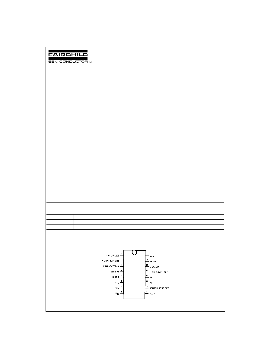
Connection Diagram
Pin Assignments for SOIC and DIP
Top View
Order Number
Package Number
Package Description
CD4046BCM
M16A
16-Lead Small Outline integrated Circuit (SOIC), JEDEC MS-012, 0.150" Narrow Body
CD4046BCN
N16E
16-Lead Plastic Dual-In-Line Package (PDIP), JEDEC MS-001, 0.300" Wide
www.fairchildsemi.com
2
C
D
40
46BC
Block Diagram
FIGURE 1.
3
www.fairchildsemi.com
CD404
6BC
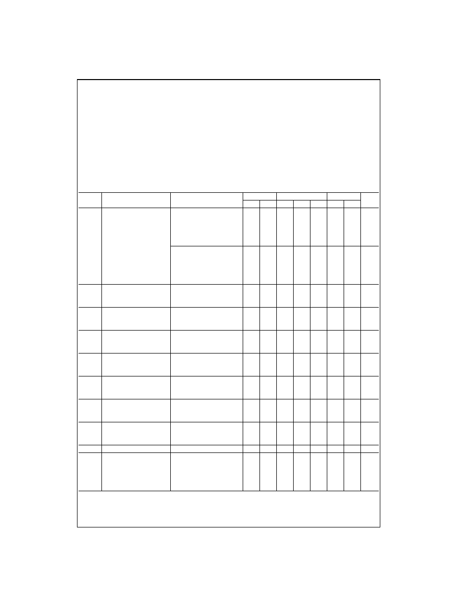
Absolute Maximum Ratings
(Note 1)
(Note 2)
Recommended Operating
Conditions
(Note 2)
Note 1: "Absolute Maximum Ratings" are those values beyond which the
safety of the device cannot be guaranteed. They are not meant to imply
that the devices should be operated at these limits. The table of "Recom-
mended Operating Conditions" and "Electrical Characteristics" provides
conditions for actual device operation.
Note 2: V
SS
=
0V unless otherwise specified.
DC Electrical Characteristics
(Note 2)
Note 3: Capacitance is guaranteed by periodic testing.
Note 4: I
OH
and I
OL
are tested one output at a time.
DC Supply Voltage (V
DD
)
-
0.5 to
+
18 V
DC
Input Voltage (V
IN
)
-
0.5 to V
DD
+
0.5 V
DC
Storage Temperature Range (T
S
)
-
65
°
C to
+
150
°
C
Power Dissipation (P
D
)
Dual-In-Line
700 mW
Small Outline
500 mW
Lead Temperature (T
L
)
(Soldering, 10 seconds)
260
°
C
DC Supply Voltage (V
DD
)
3 to 15 V
DC
Input Voltage (V
IN
)
0 to V
DD
V
DC
Operating Temperature Range (T
A
)
-
40
°
C to
+
85
°
C
Symbol
Parameter
Conditions
-
40
°
C
+
25
°
C
+
85
°
C
Units
Min
Max
Min
Typ
Max
Min
Max
I
DD
Quiescent Device Current
Pin 5
=
V
DD,
Pin 14
=
V
DD,
Pin 3, 9
=
V
SS
V
DD
=
5V
20
0.005
20
150
µ
A
V
DD
=
10V
40
0.01
40
300
µ
A
V
DD
=
15V
80
0.015
80
600
µ
A
Pin 5
=
V
DD
, Pin 14
=
Open,
Pin 3, 9
=
V
SS
V
DD
=
5V
70
5
55
205
µ
A
V
DD
=
10V
530
20
410
710
µ
A
V
DD
=
15V
1500
50
1200
1800
µ
A
V
OL
LOW Level Output Voltage
V
DD
=
5V
0.05
0
0.05
0.05
V
V
DD
=
10V
0.05
0
0.05
0.05
V
V
DD
=
15V
0.05
0
0.05
0.05
V
V
OH
HIGH Level Output Voltage
V
DD
=
5V
4.95
4.95
5
4.95
V
V
DD
=
10V
9.95
9.95
10
9.95
V
V
DD
=
15V
14.95
14.95
15
14.95
V
V
IL
LOW Level Input Voltage
V
DD
=
5V, V
O
=
0.5V or 4.5V
1.5
2.25
1.5
1.5
V
Comparator and Signal In
V
DD
=
10V, V
O
=
1V or 9V
3.0
4.5
3.0
3.0
V
V
DD
=
15V, V
O
=
1.5V or 13.5V
4.0
6.25
4.0
4.0
V
V
IH
HIGH Level Input Voltage
V
DD
=
5V, V
O
=
0.5V or 4.5V
3.5
3.5
2.75
3.5
V
Comparator and Signal In
V
DD
=
10V, V
O
=
1V or 9V
7.0
7.0
5.5
7.0
V
V
DD
=
15V, V
O
=
1.5V or 13.5V
11.0
11.0
8.25
11.0
V
I
OL
LOW Level Output Current
V
DD
=
5V, V
O
=
0.4V
0.52
0.44
0.88
0.36
mA
(Note 4)
V
DD
=
10V, V
O
=
0.5V
1.3
1.1
2.25
0.9
mA
V
DD
=
15V, V
O
=
1.5V
3.6
3.0
8.8
2.4
mA
I
OH
HIGH Level Output Current
V
DD
=
5V, V
O
=
4.6V
-
0.52
-
0.44
-
0.88
-
0.36
mA
(Note 4)
V
DD
=
10V, V
O
=
9.5V
-
1.3
-
1.1
-
2.25
-
0.9
mA
V
DD
=
15V, V
O
=
13.5V
-
3.6
-
3.0
-
8.8
-
2.4
mA
I
IN
Input Current
All Inputs Except Signal Input
V
DD
=
15V, V
IN
=
0V
-
0.3
-
10
-
5
-
0.3
-
1.0
µ
A
V
DD
=
15V, V
IN
=
15V
0.3
10
-
5
0.3
1.0
µ
A
C
IN
Input Capacitance
Any Input (Note 3)
7.5
pF
P
T
Total Power Dissipation
f
o
=
10 kHz, R1
=
1 M
,
R2
=
,
=
/2
V
DD
=
5V
0.07
mW
V
DD
=
10V
0.6
mW
V
DD
=
15V
2.4
mW
www.fairchildsemi.com
4
C
D
40
46BC
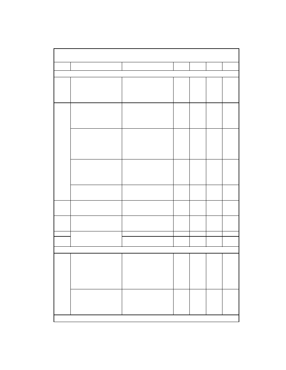
AC Electrical Characteristics
(Note 5)
T
A
=
25
°
C, C
L
=
50 pF
Symbol
Parameter
Conditions
Min
Typ
Max
Units
VCO SECTION
I
DD
Operating Current
f
o
=
10 kHz, R1
=
1 M
,
R2
=
,
=
/2
V
DD
=
5V
20
µ
A
V
DD
=
10V
90
µ
A
V
DD
=
15V
200
µ
A
f
MAX
Maximum Operating Frequency
C1
=
50 pF, R1
=
10 k
,
R2
=
,
=
V
DD
=
5V
0.4
0.8
MHz
V
DD
=
10V
0.6
1.2
MHz
V
DD
=
15V
1.0
1.6
MHz
Linearity
VCO
IN
=
2.5V
±
0.3V,
R1
10 k
, V
DD
=
5V
1
%
VCO
IN
=
5V
±
2.5V,
R1
400 k
, V
DD
=
10V
1
%
VCO
IN
=
7.5V
±
5V,
R1
1 M
, V
DD
=
15V
1
%
Temperature-Frequency Stability
%/
°
C
1/.
No Frequency Offset, f
MIN
=
0
R2
=
V
DD
=
5V
0.120.24
%/
°
C
V
DD
=
10V
0.040.08
%/
°
C
V
DD
=
15V
0.0150.03
%/
°
C
Frequency Offset, f
MIN
0
V
DD
=
5V
0.060.12
%/
°
C
V
DD
=
10V
0.050.1
%/
°
C
V
DD
=
15V
0.030.06
%/
°
C
VCO
IN
Input Resistance
V
DD
=
5V
10
6
M
V
DD
=
10V
10
6
M
V
DD
=
15V
10
6
M
VCO
Output Duty Cycle
V
DD
=
5V
50
%
V
DD
=
10V
50
%
V
DD
=
15V
50
%
t
THL
VCO Output Transition Time
V
DD
=
5V
90
200
ns
t
THL
V
DD
=
10V
50
100
ns
V
DD
=
15V
45
80
ns
PHASE COMPARATORS SECTION
R
IN
Input Resistance
Signal Input
V
DD
=
5V
1
3
M
V
DD
=
10V
0.2
0.7
M
V
DD
=
15V
0.1
0.3
M
Comparator Input
V
DD
=
5V
10
6
M
V
DD
=
10V
10
6
M
V
DD
=
15V
10
6
M
AC-Coupled Signal Input Voltage
Sensitivity
C
SERIES
=
1000 pF
f
=
50 kHz
V
DD
=
5V
200
400
mV
V
DD
=
10V
400
800
mV
V
DD
=
15V
700
1400
mV
5
www.fairchildsemi.com
CD404
6BC
AC Electrical Characteristics
(Continued)
Note 5: AC Parameters are guaranteed by DC correlated testing.
Phase Comparator State Diagrams
FIGURE 2.
Symbol
Parameter
Conditions
Min
Typ
Max
Units
DEMODULATOR OUTPUT
VCO
IN
-
V
DEM
Offset Voltage
RS
10 k
, V
DD
=
5V
1.50
2.2
V
RS
10 k
, V
DD
=
10V
1.50
2.2
V
RS
50 k
, V
DD
=
15V
1.50
2.2
V
Linearity
RS
50 k
VCO
IN
=
2.5V
±
0.3V, V
DD
=
5V
0.1
%
VCO
IN
=
5V
±
2.5V, V
DD
=
10V
0.6
%
VCO
IN
=
7.5V
±
5V, V
DD
=
15V
0.8
%
ZENER DIODE
V
Z
Zener Diode Voltage
I
Z
=
50
µ
A
6.3
7.0
7.7
V
R
Z
Zener Dynamic Resistance
I
Z
=
1 mA
100
www.fairchildsemi.com
6
C
D
40
46BC
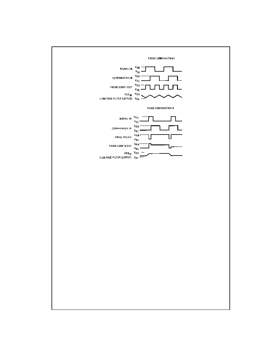
Typical Waveforms
FIGURE 3. Typical Waveform Employing Phase Comparator I in Locked Condition
FIGURE 4. Typical Waveform Employing Phase Comparator II in Locked Condition
7
www.fairchildsemi.com
CD404
6BC
Typical Performance Characteristics
Typical Center Frequency vs C1
for R1
=
10 k
, 100 k
and 1 M
FIGURE 5.
Typical Frequency vs C1
for R2
=
10 k
, 100 k
and 1 M
FIGURE 6.
Note: To obtain approximate total power dissipation of PLL system for no-signal input: Phase Comparator I, P
D
(Total)
=
P
D
(f
o
)
+
P
D
(f
MIN
)
+
P
D
(R
S
); Phase
Comparator II, P
D
(Total)
=
P
D
(f
MIN
).
www.fairchildsemi.com
8
C
D
40
46BC
Typical f
MAX
/f
MIN
vs R2/R1
FIGURE 7.
Typical VCO Power Dissipation
at Center Frequency vs R1
FIGURE 8.
Note: To obtain approximate total power dissipation of PLL system for no-signal input: Phase Comparator I, P
D
(Total)
=
P
D
(f
o
)
+
P
D
(f
MIN
)
+
P
D
(R
S
); Phase
Comparator II, P
D
(Total)
=
P
D
(f
MIN
).
9
www.fairchildsemi.com
CD404
6BC
Typical VCO Power Dissipation at f
MIN
vs R2
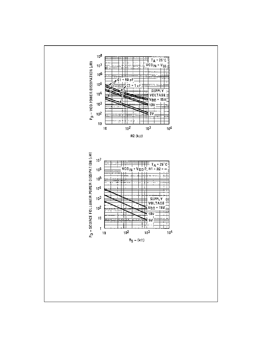
FIGURE 9.
Typical Source Follower Power Dissipation vs R
S
FIGURE 10.
Note: To obtain approximate total power dissipation of PLL system for no-signal input: Phase Comparator I, P
D
(Total)
=
P
D
(f
o
)
+
P
D
(f
MIN
)
+
P
D
(R
S
); Phase
Comparator II, P
D
(Total)
=
P
D
(f
MIN
).
www.fairchildsemi.com
10
C
D
40
46BC
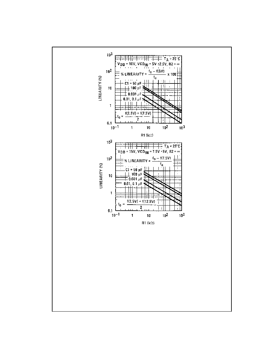
FIGURE 11. Typical VCO Linearity vs R1 and C1
Note: To obtain approximate total power dissipation of PLL system for no-signal input: Phase Comparator I, P
D
(Total)
=
P
D
(f
o
)
+
P
D
(f
MIN
)
+
P
D
(R
S
); Phase
Comparator II, P
D
(Total)
=
P
D
(f
MIN
).
11
www.fairchildsemi.com
CD404
6BC
Design Information
This information is a guide for approximating the value of
external components for the CD4046B in a phase-locked-
loop system. The selected external components must be
within the following ranges: R1, R2
10 k
, R
S
10 k
,
C1
50 pF.
In addition to the given design information, refer to Figure
5, Figure 6, Figure 7 for R1, R2 and C1 component selec-
tions.
Using Phase Comparator I
Using Phase Comparator II
Characteristics
VCO Without Offset
VCO With Offset
VCO Without Offset
VCO With Offset
R2
=
R2
=
VCO Frequency
For No Signal Input
VCO in PLL system will adjust
VCO in PLL system will adjust to
to center frequency, f
o
lowest operating frequency, f
min
Frequency Lock
2 f
L
=
full VCO frequency range
Range, 2 f
L
2 f
L
=
f
max
-
f
min
Frequency Capture
Range, 2 f
C
Loop Filter Component
Selection
For 2 f
C
, see Ref.
f
C
=
f
L
Phase Angle Between
90
°
at center frequency (f
o
), approximating
Always 0
°
in lock
Single and Comparator
0
°
and 180
°
at ends of lock range (2 f
L
)
Locks on Harmonics
Yes
No
of Center Frequency
Signal Input Noise
High
Low
Rejection
www.fairchildsemi.com
12
C
D
40
46BC
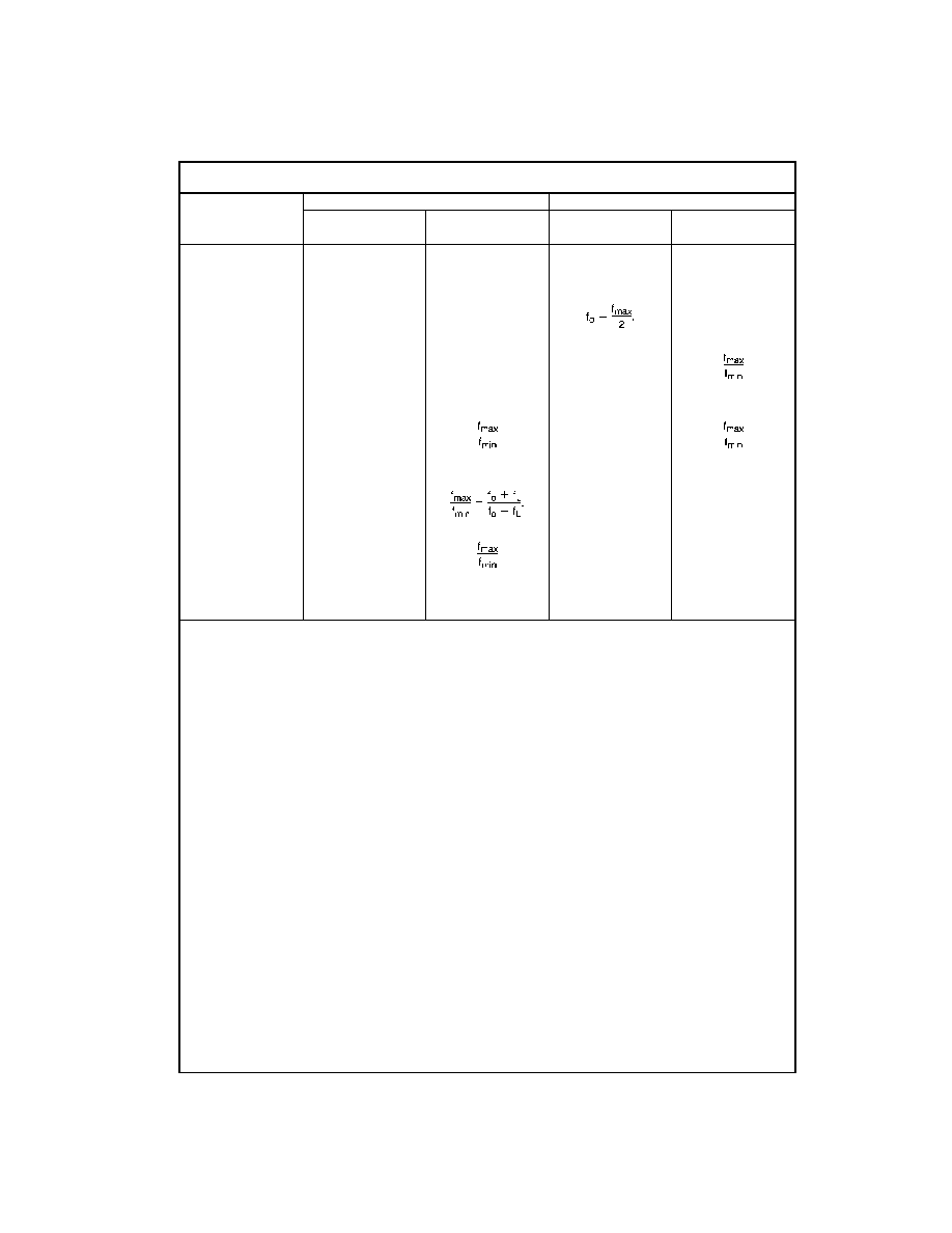
References
G.S. Moschytz, "Miniaturized RC Filters Using Phase-Locked Loop", BSTJ, May, 1965.
Floyd Gardner, "Phaselock Techniques", John Wiley & Sons, 1966.
Using Phase Comparator I
Using Phase Comparator II
Characteristics
VCO Without Offset
VCO With Offset
VCO Without Offset
VCO With Offset
R2
=
R2
=
VCO Component
Selection
Given: f
o
.
Given: f
o
and f
L
.
Given: f
max
.
Given: f
min
and f
max
.
Use f
o
with
Calculate f
min
Calculate f
o
from
Use f
min
with
Figure 5 to
from the equation
the equation
Figure 6 to
determine R1 and C1.
f
min
=
f
o
-
f
L
.
to determine R2 and
C1.
Use f
min
with Figure 6 to
determine R2 and C1.
Calculate
Use f
o
with Figure 5 to
Calculate
determine R1 and C1.
Use
with Figure 7
from the equation
to determine ratio
R2/R1 to obtain R1.
Use
with Figure 7
to determine ratio R2/
R1 to obtain R1.
13
www.fairchildsemi.com
CD404
6BC
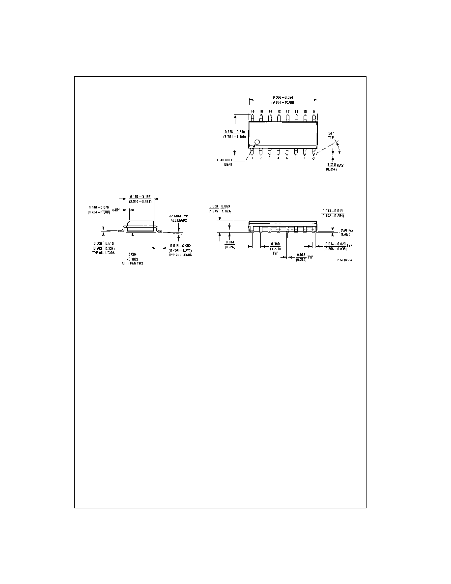
Physical Dimensions
inches (millimeters) unless otherwise noted
16-Lead Small Outline Integrated Circuit (SOIC), JEDEC MS-012, 0.150" Narrow Body
Package Number M16A
Fairchild does not assume any responsibility for use of any circuitry described, no circuit patent licenses are implied and Fairchild reserves the right at any time without notice to change said circuitry and specifications.
CD4046BC Micr
opo
wer Phase-L
o
c
ked
Loo
p
LIFE SUPPORT POLICY
FAIRCHILD'S PRODUCTS ARE NOT AUTHORIZED FOR USE AS CRITICAL COMPONENTS IN LIFE SUPPORT
DEVICES OR SYSTEMS WITHOUT THE EXPRESS WRITTEN APPROVAL OF THE PRESIDENT OF FAIRCHILD
SEMICONDUCTOR CORPORATION. As used herein:
1. Life support devices or systems are devices or systems
which, (a) are intended for surgical implant into the
body, or (b) support or sustain life, and (c) whose failure
to perform when properly used in accordance with
instructions for use provided in the labeling, can be rea-
sonably expected to result in a significant injury to the
user.
2. A critical component in any component of a life support
device or system whose failure to perform can be rea-
sonably expected to cause the failure of the life support
device or system, or to affect its safety or effectiveness.
www.fairchildsemi.com
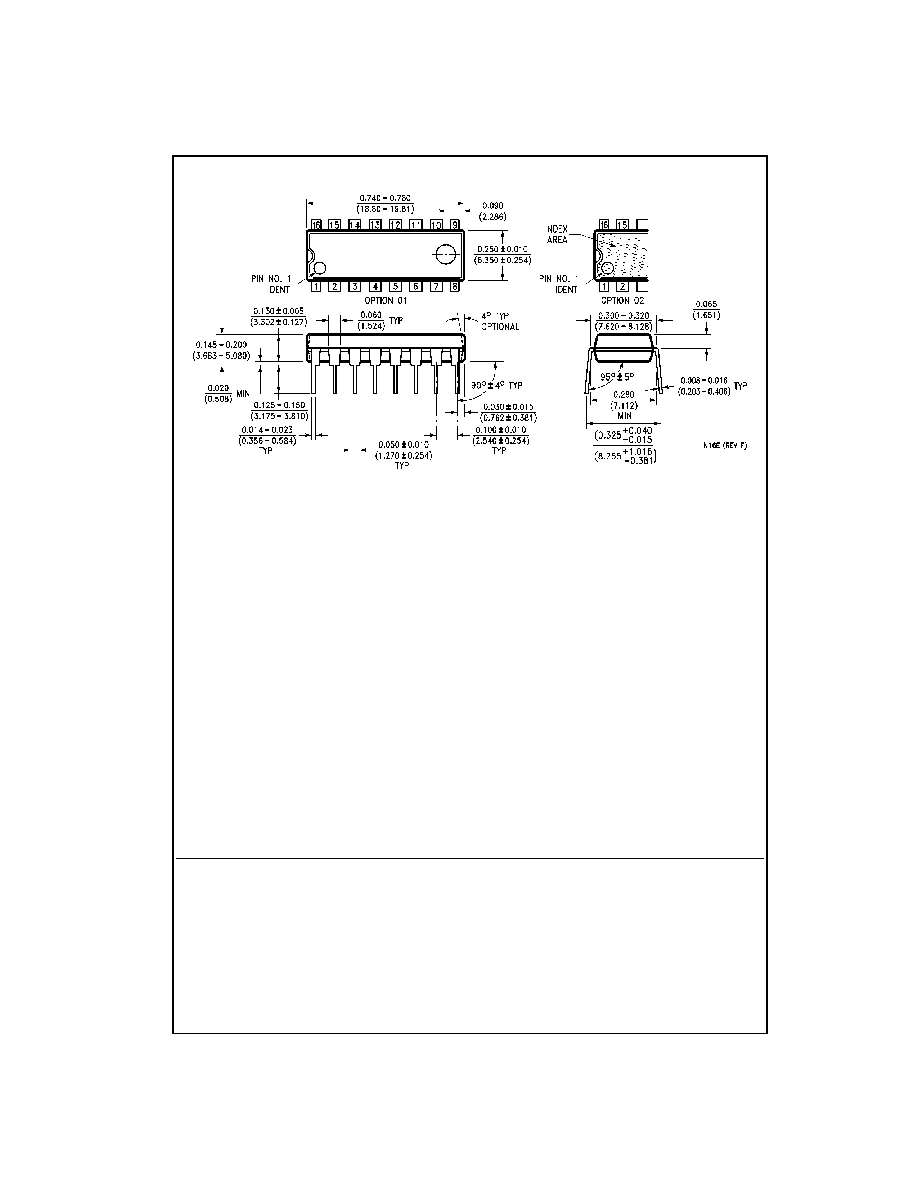
Physical Dimensions
inches (millimeters) unless otherwise noted (Continued)
16-Lead Plastic Dual-In-Line Package (PDIP), JEDEC MS-001, 0.300" Wide
Package Number N16E