October 1987
Revised January 1999
CD453
8BC
Dual
Prec
isi
on Monost
ab
l
e
© 1999 Fairchild Semiconductor Corporation
DS006000.prf
www.fairchildsemi.com
CD4538BC
Dual Precision Monostable
General Description
The CD4538BC is a dual, precision monostable multivibra-
tor with independent trigger and reset controls. The device
is retriggerable and resettable, and the control inputs are
internally latched. Two trigger inputs are provided to allow
either rising or falling edge triggering. The reset inputs are
active LOW and prevent triggering while active. Precise
control of output pulse-width has been achieved using lin-
ear CMOS techniques. The pulse duration and accuracy
are determined by external components R
X
and C
X
. The
device does not allow the timing capacitor to discharge
through the timing pin on power-down condition. For this
reason, no external protection resistor is required in series
with the timing pin. Input protection from static discharge is
provided on all pins.
Features
s
Wide supply voltage range:
3.0V to 15V
s
High noise immunity:
0.45 V
CC
(typ.)
s
Low power TTL compatibility:
Fan out of 2 driving 74L
or 1 driving 74LS
s
New formula: PW
OUT
=
RC (PW in seconds, R in Ohms,
C in Farads)
s
±
1.0% pulse-width variation from part to part (typ.)
s
Wide pulse-width range:
1
µ
s to
s
Separate latched reset inputs
s
Symmetrical output sink and source capability
s
Low standby current:
5 nA (typ.) @ 5 V
DC
s
Pin compatible to CD4528BC
Ordering Code:
Devices also available in Tape and Reel. Specify by appending the suffix letter "X" to the ordering code.
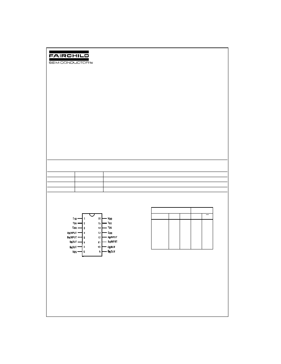
Connection Diagram
Pin Assignments for DIP and SOIC
Top View
Truth Table
H
=
HIGH Level
L
=
LOW Level
=
Transition from LOW-to-HIGH
=
Transition from HIGH-to-LOW
�
=
One HIGH Level Pulse
=
One LOW Level Pulse
X
=
Irrelevant
Order Number
Package Number
Package Description
CD4538BCM
M16A
16-Lead Small Outline Integrated Circuit (SOIC), JEDEC MS-012, 0.150" Narrow Body
CD4538BCWM
M16B
16-Lead Small Outline Integrated Circuit (SOIC), JEDEC MS-013, 0.300" Wide Body
CD4538BCN
N16E
16-Lead Plastic Dual-In-Line Package (PDIP), JEDEC MS-001, 0.300" Wide
Inputs
Outputs
Clear
A
B
Q
Q
L
X
X
L
H
X
H
X
L
H
X
X
L
L
H
H
L
�
H
H
�
3
www.fairchildsemi.com
CD453
8BC
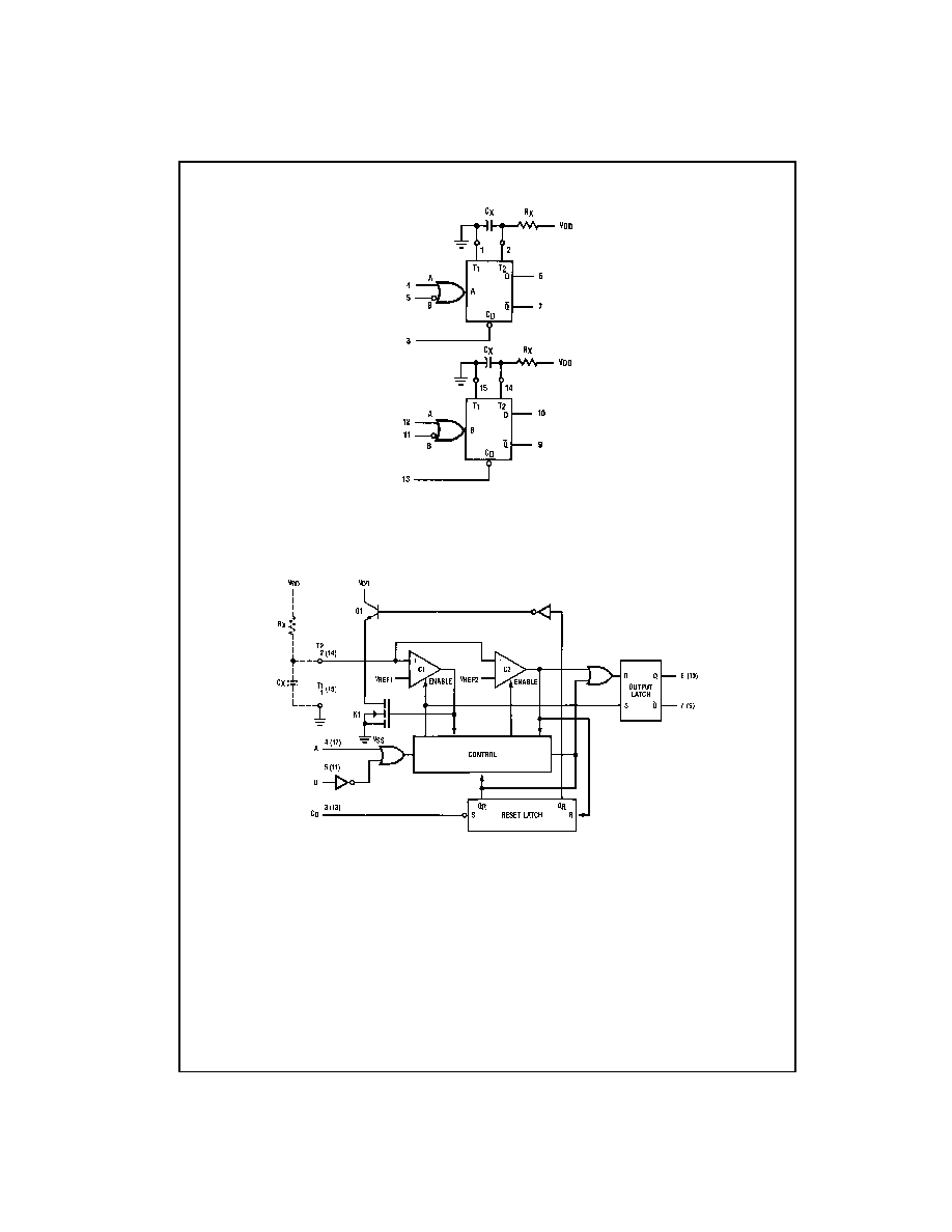
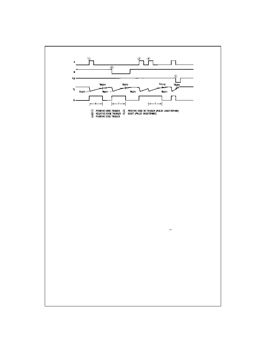
Theory of Operation
FIGURE 2.
Trigger Operation
The block diagram of the CD4538BC is shown in Figure 1,
with circuit operation following.
As shown in Figure 1 and Figure 2, before an input trigger
occurs, the monostable is in the quiescent state with the Q
output low, and the timing capacitor C
X
completely charged
to V
DD
. When the trigger input A goes from V
SS
to V
DD
(while inputs B and C
D
are held to V
DD
) a valid trigger is
recognized, which turns on comparator C1 and N-Channel
transistor N1
(1)
. At the same time the output latch is set.
With transistor N1 on, the capacitor C
X
rapidly discharges
toward V
SS
until V
REF1
is reached. At this point the output
of comparator C1 changes state and transistor N1 turns off.
Comparator C1 then turns off while at the same time com-
parator C2 turns on. With transistor N1 off, the capacitor C
X
begins to charge through the timing resistor, R
X
, toward
V
DD
. When the voltage across C
X
equals V
REF2
, compara-
tor C2 changes state causing the output latch to reset (Q
goes low) while at the same time disabling comparator C2.
This ends the timing cycle with the monostable in the qui-
escent state, waiting for the next trigger.
A valid trigger is also recognized when trigger input B goes
from V
DD
to V
SS
(while input A is at V
SS
and input C
D
is at
V
DD
)
(2)
.
It should be noted that in the quiescent state C
X
is fully
charged to V
DD
, causing the current through resistor R
X
to
be zero. Both comparators are "off" with the total device
current due only to reverse junction leakages. An added
feature of the CD4538BC is that the output latch is set via
the input trigger without regard to the capacitor voltage.
Thus, propagation delay from trigger to Q is independent of
the value of C
X
, R
X
, or the duty cycle of the input wave-
form.
Retrigger Operation
The CD4538BC is retriggered if a valid trigger occurs
(3)
fol-
lowed by another valid trigger
(4)
before the Q output has
returned to the quiescent (zero) state. Any retrigger, after
the timing node voltage at pin 2 or 14 has begun to rise
from V
REF1
, but has not yet reached V
REF2
, will cause an
increase in output pulse width T. When a valid retrigger is
initiated
(4)
, the voltage at T2 will again drop to V
REF1
before
progressing along the RC charging curve toward V
DD
. The
Q output will remain high until time T, after the last valid
retrigger.
Reset Operation
The CD4538BC may be reset during the generation of the
output pulse. In the reset mode of operation, an input pulse
on C
D
sets the reset latch and causes the capacitor to be
fast charged to V
DD
by turning on transistor Q1
(5)
. When
the voltage on the capacitor reaches V
REF2
, the reset latch
will clear and then be ready to accept another pulse. If the
C
D
input is held low, any trigger inputs that occur will be
inhibited and the Q and Q outputs of the output latch will
not change. Since the Q output is reset when an input low
level is detected on the C
D
input, the output pulse T can be
made significantly shorter than the minimum pulse width
specification.
5
www.fairchildsemi.com
CD453
8BC
Absolute Maximum Ratings
(Note 1)
(Note 2)
Recommended Operating
Conditions
(Note 2)
Note 1: "Absolute Maximum Ratings" are those values beyond which the
safety of the device cannot be guaranteed, they are not meant to imply that
the devices should be operated at these limits. The tables of "Recom-
mended Operating Conditions" and "Electrical Characteristics" provide con-
ditions for actual device operation.
Note 2: V
SS
=
0V unless otherwise specified.
DC Electrical Characteristics
(Note 2)
Note 3: I
OH
and I
OL
are tested one output at a time.
DC Supply Voltage (V
DD
)
-
0.5 to
+
18 V
DC
Input Voltage (V
IN
)
-
0.5V to V
DD
+
0.5 V
DC
Storage Temperature Range (T
S
)
-
65
∞
C to
+
150
∞
C
Power Dissipation (P
D
)
Dual-In-Line
700 mW
Small Outline
500 mW
Lead Temperature (T
L
)
(Soldering, 10 seconds)
260
∞
C
DC Supply Voltage (V
DD
)
3 to 15 V
DC
Input Voltage (V
IN
)
0 to V
DD
V
DC
Operating Temperature Range (T
A
)
-
40
∞
C to
+
85
∞
C
Symbol
Parameter
Conditions
-
40
∞
C
+
25
∞
C
+
85
∞
C
Units
Min
Max
Min
Typ
Max
Min
Max
I
DD
Quiescent
V
DD
=
5V
V
IH
=
V
DD
20
0.005
20
150
µ
A
Device Current
V
DD
=
10V
V
IL
=
V
SS
40
0.010
40
300
µ
A
V
DD
=
15V
All Outputs Open
80
0.015
80
600
µ
A
V
OL
LOW Level
V
DD
=
5V
|I
O
|
<
1
µ
A
0.05
0
0.05
0.05
V
Output Voltage
V
DD
=
10V
V
IH
=
V
DD
, V
IL
=
V
SS
0.05
0
0.05
0.05
V
V
DD
=
15V
0.05
0
0.05
0.05
V
V
OH
HIGH Level
V
DD
=
5V
|I
O
|
<
1
µ
A
4.95
4.95
5
4.95
V
Output Voltage
V
DD
=
10V
V
IH
=
V
DD
, V
IL
=
V
SS
9.95
9.95
10
9.95
V
V
DD
=
15V
14.95
14.95
15
14.95
V
V
IL
LOW Level
|I
O
|
<
1
µ
A
Input Voltage
V
DD
=
5V, V
O
=
0.5V or 4.5V
1.5
2.25
1.5
1.5
V
V
DD
=
10V, V
O
=
1.0V or 9.0V
3.0
4.50
3.0
3.0
V
V
DD
=
15V, V
O
=
1.5V or 13.5V
4.0
6.75
4.0
4.0
V
V
IH
HIGH Level
|I
O
|
<
1
µ
A
Input Voltage
V
DD
=
5V, V
O
=
0.5V or 4.5V
3.5
3.5
2.75
3.5
V
V
DD
=
10V, V
O
=
1.0V or 9.0V
7.0
7.0
5.50
7.0
V
V
DD
=
15V, V
O
=
1.5V or 13.5V
11.0
11.0
8.25
11.0
V
I
OL
LOW Level
V
DD
=
5V, V
O
=
0.4V
V
IH
=
V
DD
0.52
0.44
0.88
0.36
mA
Output Current
V
DD
=
10V, V
O
=
0.5V
V
IL
=
V
SS
1.3
1.1
2.25
0.9
mA
(Note 3)
V
D
=
15V, V
O
=
1.5V
3.6
3.0
8.8
2.4
mA
I
OH
HIGH Level
V
DD
=
5V, V
O
=
4.6V
-
0.52
-
0.44
-
0.88
-
0.36
mA
Output Current
V
DD
=
10V, V
O
=
9.5V
V
IL
=
V
SS
-
1.3
-
1.1
-
2.25
-
0.9
mA
(Note 3)
V
D
=
15V, V
O
=
13.5V
-
3.6
-
3.0
-
8.8
-
2.4
mA
I
IN
Input Current,
V
DD
=
15V, V
IN
=
0V or 15V
±
0.02
±
10
-
5
±
0.05
±
0.5
µ
A
Pin 2 or 14
I
IN
Input Current
V
DD
=
15V, V
IN
=
0V or 15V
±
0.3
±
10
-
5
±
0.3
±
1.0
µ
A
Other Inputs