Äîêóìåíòàöèÿ è îïèñàíèÿ www.docs.chipfind.ru
©2000 Fairchild Semiconductor International
www.fairchildsemi.com
Rev. 1.0.1
Oct. 2000.
Features
· 3-phase, full-wave, linear BLDC motor driver
· Power save at stop mode
· Built-in current limiter
· Built-in TSD (Thermal shutdown) circuit
· Built-in 3X and 1X hall FG output
· Built-in hall bias circuit
· Built-in rotational direction detector
· Built-in reverse rotation preventer
· Built-in short braker
· Corresponds to 3.3V DSP
Description
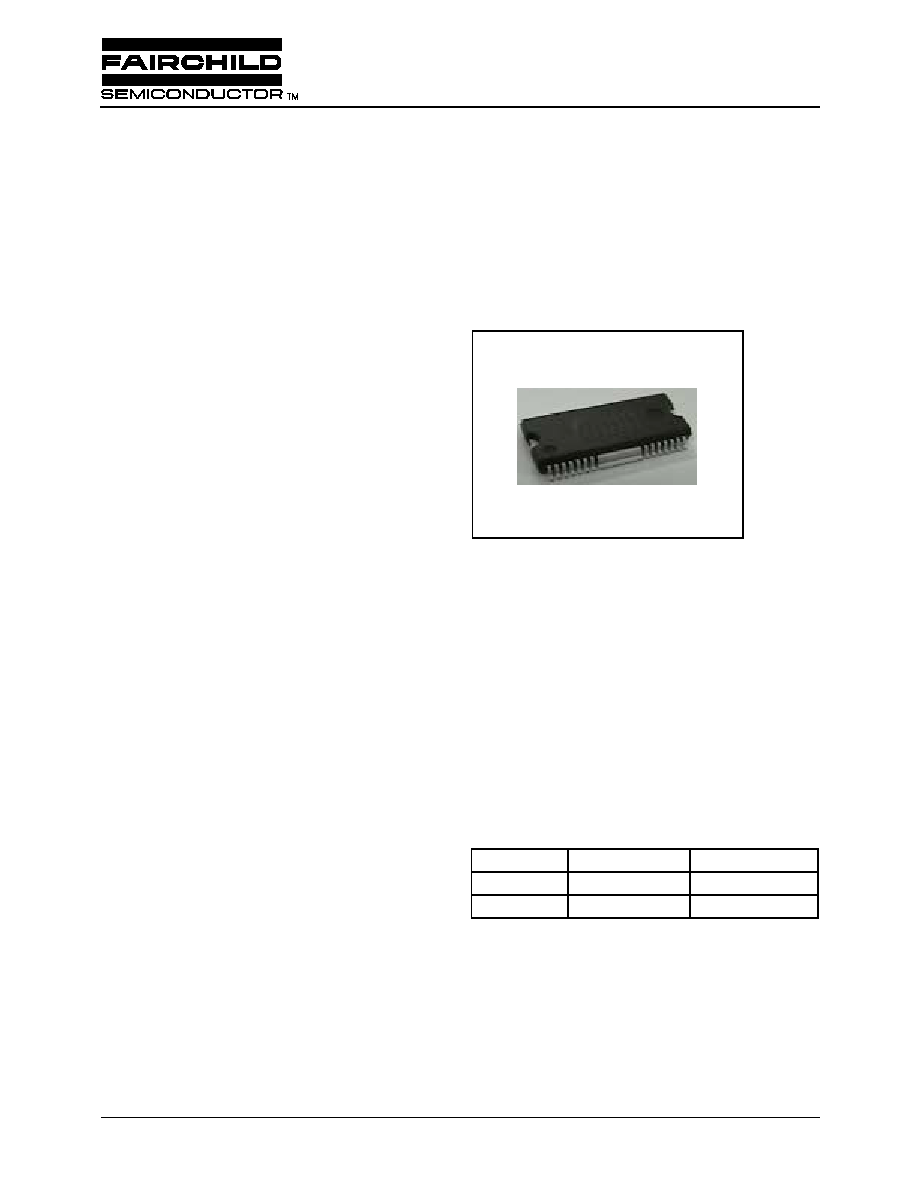
The FAN8420D3 is a monolithic IC, suitable for a 3-phase
spindle motor driver of a CD-media system.
28-SSOPH-375
28-SSOPH-375SG2
Typical Applications
· Compact disk ROM (CD-ROM) spindle motor
· Compact disk RW (CD-RW) spindle motor
· Digital video disk ROM (DVD-ROM) spindle motor
· Digital video disk RAM (DVD-RAM) spindle motor
· Digital video disk Player (DVDP) spindle motor
· Other compact disk media spindle motor
· Other 3-phase BLDC motor
Ordering Information
Device
Package
Operating Temp.
FAN8420D3
28-SSOPH-375SG2
-
25
°
C ~ +75
°
C
FAN8420D3TF 28-SSOPH-375SG2
-
25
°
C ~ +75
°
C
FAN8420D3
3-Phase BLDC Motor Driver
FAN8420D3
2
Rev. 1.0.1
Oct.. 2000.
Pin Assignments
Pin Definitions
Pin Number
Pin Name
I/O
Pin Function Description
1
NC
-
No connection
2
A3
O
Output (A3)
3
NC
-
No connection
4
A2
O
Output (A2)
5
NC
-
No connection
6
NC
-
No connection
7
A1
O
Output (A1)
8
GND
-
Ground
9
H1+
I
Hall signal (H1+)
10
H1
-
I
Hall signal (H1
-
)
11
H2+
I
Hall signal (H2+)
12
H2
-
I
Hall signal (H2
-
)
13
H3+
I
Hall signal (H3+)
14
H3
-
I
Hall signal (H3
-
)
15
VH
I
Hall bias
16
NC
-
No connection
17
PC1
-
Phase compensation capacitor
18
SB
I
Short brake
19
FG3X
O
FG waveform (3X)
20
DIR
O
Rotational direction output
21
ECR
I
Output current control reference
22
EC
I
Output current control voltage
1
2
3
4
5
6
7
8
9
10
11
12
13
14
15
16
17
18
19
20
21
22
23
24
25
26
27
28
FAN8420D3
NC
A3
NC
A2
NC
A1
NC
GND
H1
+
H1
-
H2
+
H2
-
H3
+
H3
-
CS1
VM
NC
VCC
S/
S
EC
FG1X
ECR
DI
R
FG3X
SB
PC1
NC
VH
FIN(GND)
FIN(GND)
FAN8420D3
3
Rev. 1.0.1
Oct. 2000.
Pin Definitions (Continued)
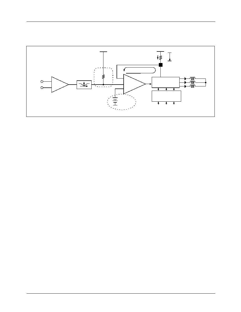
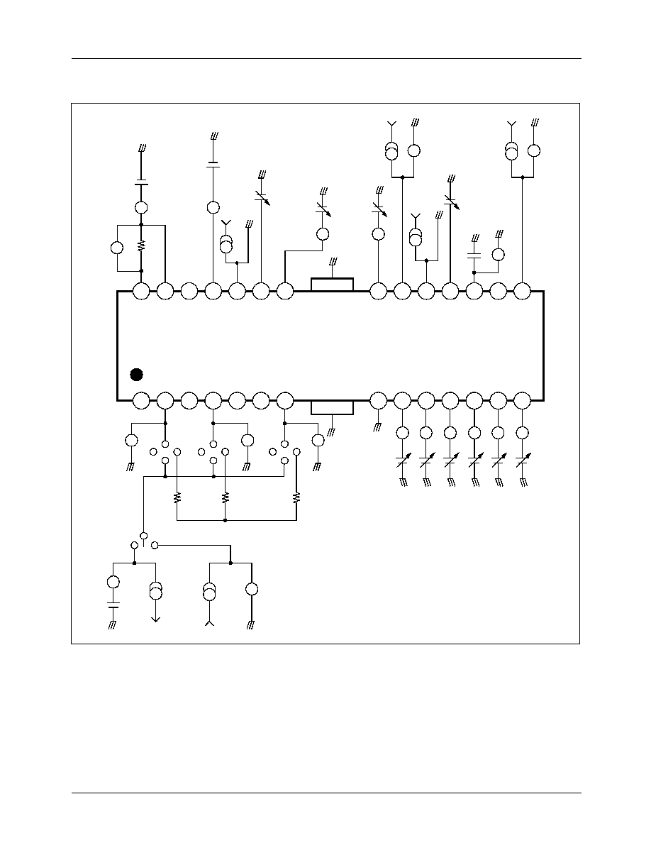
Internal Block Diagram
Pin Number
Pin Name
I/O
Pin Function Description
23
S/S
I
Power save (Start/Stop switch)
24
FG1X
O
FG waveform (1X)
25
VCC
-
Supply voltage (Signal)
26
NC
-
No connection
27
VM
-
Supply voltage (Motor)
28
CS1
-
Output current detection
1
2
3
4
5
6
7
8
9
10
11
12
13
14
15
16
17
18
19
20
21
22
23
24
25
26
27
28
FG
1X
Gener
at
or
St
a
r
t
St
op
Sh
or
t
Br
a
k
e
R
e
ve
r
s
e
r
o
ta
tio
n
C
o
m
m
ut
at
i
o
n
Sel
e
ct
or
De
t
e
ct
or
De
t
e
ct
i
o
n
Upp
e
r
Di
s
t
r
i
but
or
Lower
Di
st
r
i
b
u
t
o
r
Hall amp
TSD
Hal
l
Absolute
Values
Current sense
Amp
Output
Current limit
+
-
NC
A3
NC
A2
NC
NC
A1
GN
D
H1+
H1
-
H2+
H2
-
H3+
H3
-
VH
NC
SB
PC1
FG
3X
DI
R
ECR
EC
S/
S
FG
1X
VCC
NC
VM
CS1
Lo
gi
c
Gen
e
r
a
t
o
r
FG3X
GND
GND
FAN8420D3
4
Rev. 1.0.1
Oct.. 2000.
Equivalent Circuits
Hall input
Driver output
Torque control input
Hall bias input
Start / Stop input
Short brake input
FG output
Dir output
1k
11
9
13
12
14
10
1k
50
50
28
2
27
4
7
+
-
21
22
50
50
15
100k
23
40k
30k
50
18
1k
20k
50
10k
V
CC
24
50
19
30k
V
CC
20
50
FAN8420D3
5
Rev. 1.0.1
Oct. 2000.
Absolute Maximum Ratings
(Ta = 25
°
°
°
°
C)
NOTE:
1. When mounted on a 76.2mm
×
114mm
×
1.57mm PCB (Phenolic resin material).
2. Power dissipation reduces 16.6mW/
°
°
°
°
C for using above Ta = 25
°
°
°
°
C
3. Do not exceed P
D
and SOA (Safe operating area).
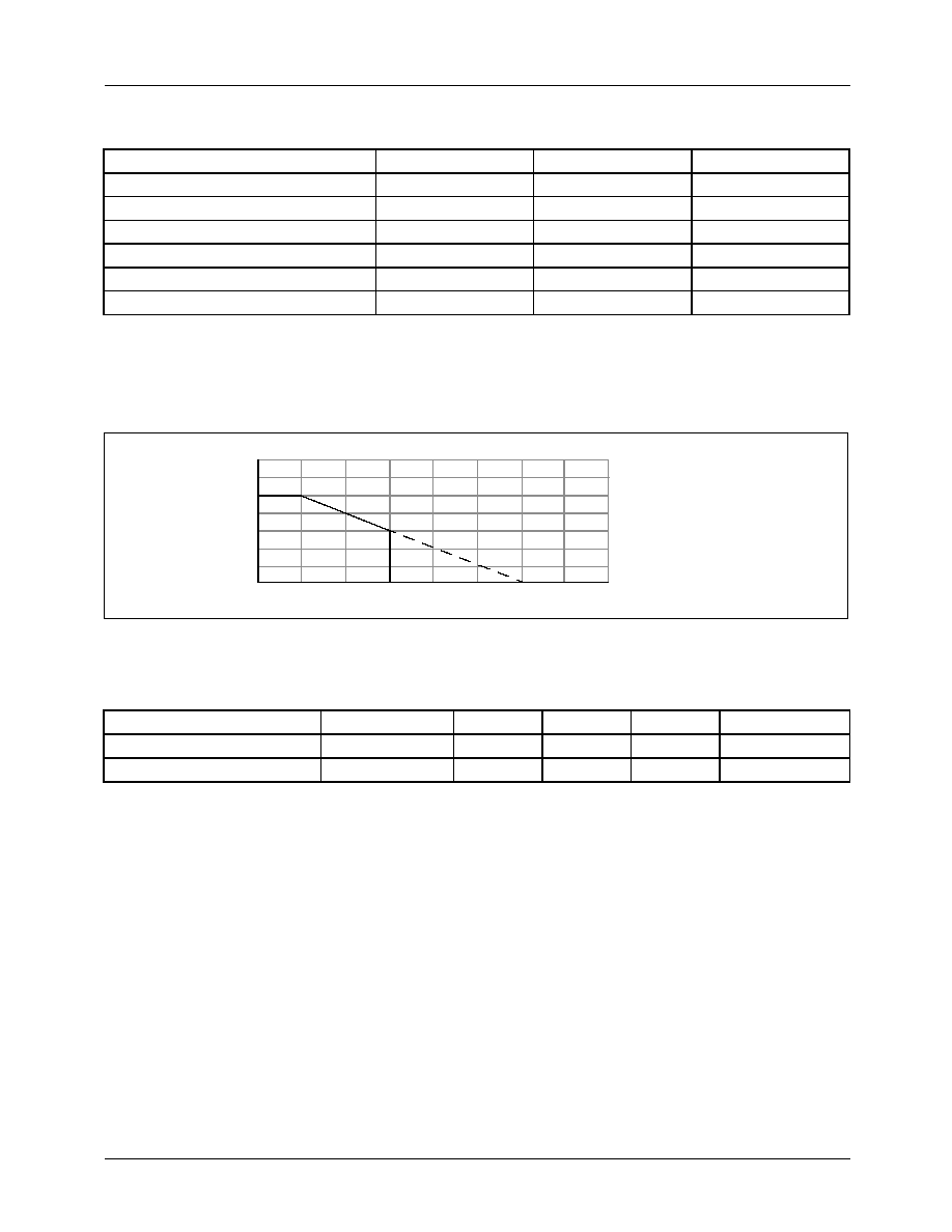
Power Dissipation Curve
Recommended Operating Conditions (Ta = 25
°
°
°
°
C)
Parameter
Symbol
Value
Unit
Maximum supply voltage (Signal)
V
CCmax
7
V
Maximum supply voltage (Motor)
V
Mmax
15
V
Power dissipation
P
D
2.5
note
W
Maximum output current
I
Omax
1.3
A
Operating temperature range
T
OPR
-
25 ~ +75
°
C
Storage temperature range
T
STG
-
55 ~ +150
°
C
Parameter
Symbol
Min.
Typ.
Max.
Unit
Supply voltage
V
CC
4.5
5
5.5
V
Motor supply voltage
V
M
3.0
12
14
V
3,000
2,000
1,000
0
0
25
50
75
100
125
150
175
Pd (mW)
Ambient temperature, Ta [
°
C]
SOA
FAN8420D3
6
Rev. 1.0.1
Oct.. 2000.
Electrical Characteristics
(Unless otherwise specified, Ta=25
°
C, V
CC
=5V, V
M
=12V)
Parameter
Symbol
Conditions
Min.
Typ.
Max.
Unit
Quiescent circuit current 1
I
CC1
At stop mode
-
-
0.2
mA
Quiescent circuit current 2
I
CC2
At start mode
-
5
10
mA
START / STOP
On voltage range
V
SSon
Output driver on
2.5
-
V
CC
V
Off voltage range
V
SSoff
Output driver off
0.0
-
1.0
V
HALL BIAS
Hall bias voltage
V
HB
I
HB
=20mA
0.4
1.0
1.8
V
HALL AMP
Hall bias current
I
HA
-
-
0.5
2
µ
A
Common-mode input range
V
HAR
-
1.0
-
4.0
V
Minimum input level
V
INH
-
60
-
-
mVpp
H1 hysteresis level
V
HYS
-
5
20
40
mVpp
TORQUE CONTROL
Ecr Input voltage range
E
CR
-
0.2
-
3.3
V
Ec Input voltage range
E
C
-
0.2
-
3.3
V
Offset voltage (
-
)
E
Coff
-
E
C
=1.9V
-
80
-
50
-
20
mV
Offset voltage (+)
E
Coff+
E
C
=1.9V
20
50
80
mV
Ec Input current
E
Cin
E
C
=1.9V
-5
-0.5
-
µ
A
Ecr Input current
E
CRin
E
CR
=1.9V
-5
-0.5
-
µ
A
Input / output gain
G
EC
E
C
=1.9V, R
CS
=0.5
0.56
0.71
0.84
A/V
FG
FG output voltage (H)
V
FGh
Ifg=-10
µ
A
4.5
4.9
-
V
FG output voltage (L)
V
FGl
Ifg=10
µ
A
-
-
0.5
V
Duty (reference value)
-
-
50
-
%
OUTPUT BLOCK
Saturation voltage (upper TR)
V
OH
I
O
=
-
300mA
-
0.9
1.4
V
Saturation voltage (lower TR)
V
OL
I
O
=300mA
-
0.4
0.7
V
Torque limit current
I
TL
R
CS
=0.5
560
700
840
mA
DIRECTION DETECTOR
Dir output voltage (H)
V
DIRh
Ifg=-10
µ
A
4.5
4.7
-
V
Dir output voltage (L)
V
DIRl
Ifg=10
µ
A
-
-
0.5
V
SHORT BRAKE
On voltage range
V
SBon
-
2.5
-
V
CC
V
Off voltage range
V
SBoff
-
0
-
1.0
V
FAN8420D3
7
Rev. 1.0.1
Oct. 2000.
Electrical Characteristics (Continued)
1. Calculation Of Gain & Torque Limit Current
0.355 is GM times R1 and is a fixed value within IC.
Vmax (see above block diagram) is set at 350mV.
EC
ECR
+
-
Gm
-
+
+
Absolute
Values
Current / Voltage
Convertor
R1
Vin
+
-
Driver
VM
Vmax
Max. output current limiting
+
-
VM
VM
Negative
Feedback loop
I
O
R
S
V
S
-
+
CS1 (Pin 28)
Output
Current sense
Power
Transistors
Commutation
Distributor
U
V
W
H1
H2
H3
I
O
Gain
0.355
R
S
---------------
A V
/
[
]
=
Itl
Vmax
R
S
----------------
350 mV
[
]
R
S
------------------------
=
=
FAN8420D3
8
Rev. 1.0.1
Oct.. 2000.
Application Information
1. Torque Control & Output Current Control
· By amplifying the voltage difference between E
C
and Ecr from servo IC, the torque sense amp produces the input (V
AMP
)
for the current sense amp.
· The output current (I
O
) is converted into the voltage (V
CS
) through the sense resistor (R
CS
) and compared with the V
AMP
.
By the negative feedback loop, the sensed output voltage, V
CS
is equal to the input V
AMP
. Therefore, the output current
(I
O
) is linearly controlled by the input V
AMP
.
· As a result, the signals, E
C
and E
CR
can control the velocity of the Motor by controlling the output current (I
O
) of the
driver.
· The range of the torque voltage is as shown below.
+
-
-
-
-
+
-
-
-
-
Torque AMP
E
C
E
CR
V
M
ECR-EC
Current Sense AMP
TSD
Gain
Controller
Driver
M
R
CS
V
CS
+
-
I
O
V
M
Forward
Ecoff+
Ecoff-
Reverse
Current
[mA]
6
0
E
CR
-E
C
Rotation
E
CR
> Ec
Forward rotation
E
CR
< Ec
Stop after detecting re-
verse rotation
The input range of E
CR
and E
C
is 0.2 V ~ 3.3 V ( R
NF
= 0.5[
] )
500
700
50mV
-50mV
0.71[A/V]
FAN8420D3
9
Rev. 1.0.1
Oct. 2000.
2. Short Brake
When the pick-up mechanism moves from the inner to the outer spindle of the CD, the brake function of the reverse voltage is
commonly employed to decrease the rotating velocity of the spindle Motor.
However, if the spindle motor rotates rapidly, the brake function of the reverse voltage may produce more heat at the Drive IC.
To remove this shortcoming and to enhance the braking efficiency, the short brake function is added to FAN8420D3. When the
short brake function is active, all upper power TRs turn off and all lower power TRs turn on, and the motor slows down. But
FG and DIR functions continue to operate normally.
3. Power Save
When power save function is active, all power TRs turn off.
Pin # 18
Short brake
High
On
Low
Off
Pin # 23
Start/Stop
High
Operate
Low
Stop
2
4
7
18
V
CC
ON
OFF
20k
1k
MOTOR
OFF
ON
Start
Stop
2
4
7
23
V
CC
30k
40k
MOTOR
OFF
OFF
FAN8420D3
10
Rev. 1.0.1
Oct.. 2000.
4. Tsd (Thermal Shutdown)
When the chip temperature rises above 175
°
C, the Q2 turns on and the output driver shuts down. When the chip temperature
falls off to about 150
°
C, then the Q2 turns off and the driver operates normally. TSD has the temperature hysteresis of about
25
°
C.
5. Rotational Direction Detection
· The forward and the reverse rotations of the CD are detected by the D-F/F and the truth table is shown in the above.
· The rotational direction of the CD can be explained by the output waveforms of the Hall sensors. The three outputs of Hall
sensors be H1, H2 and H3 respectively.
When the spindle rotates in reverse direction, the Hall sensor output waveforms are shown in Fig.(a). The phases order are
in H1
H2
H3 with a 120
°
C phase difference.
On the other hand, if the spindle rotates in forward rotation, the phase relationship is H3
H2
H1 as shown in fig.(b)
Gain
Controller
BIAS
Q2
20
+
-
+
-
V
CC
DIR
D-F/F
D
Q
CK
H2+
H3+
H3
-
H2
-
Rotation
DIR
Forward
Low
Reverse
High
20
(a) Reverse rotation
H1
H2
H3
FAN8420D3
11
Rev. 1.0.1
Oct. 2000.
Therefore, the output of the rotational direction detector is low, when the spindle rotates forward, and high in the reverse rota-
tion.
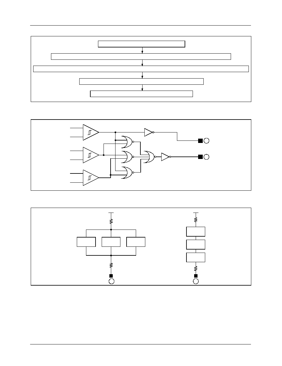
6. Reverse Rotation Prevention
· When the output of the OR Gate, A is LOW, it steers all the output current of the current sense Amp to the Gain Controller
zero. The output current of the Driver becomes zero and the motor stops.
· As in the state of the forward rotation, the D-F/F output, Q is HIGH and the motor rotates normally. At this state, if the
control input is changed such that EC>ECR, then the motor rotates slowly by the reverse commutation in the Driver. When
the motor rotates in reverse direction, the D-F/F output becomes Low and the OR Gate output, becomes LOW. This
prevents the motor from rotating in reverse direction. The operation principle is shown in the table and the flow chart.
Rotation
H2
H3
D-F/F(Q)
Reverse rotation preventer
E
C
<E
CR
E
C
>E
CR
Forward
H
H
L
H
Forward
-
Reverse
L
H
L
L
-
Brake and stop
(b) Forward rotation
H1
H2
H3
+
-
+
-
+
-
Current
Sense
Amp
Gain
Controller
Driver
D-F/F
M
D
Q
CK
H3+
H3
-
H2+
H2
-
E
C
E
CR
A
Low Active
FAN8420D3
12
Rev. 1.0.1
Oct.. 2000.
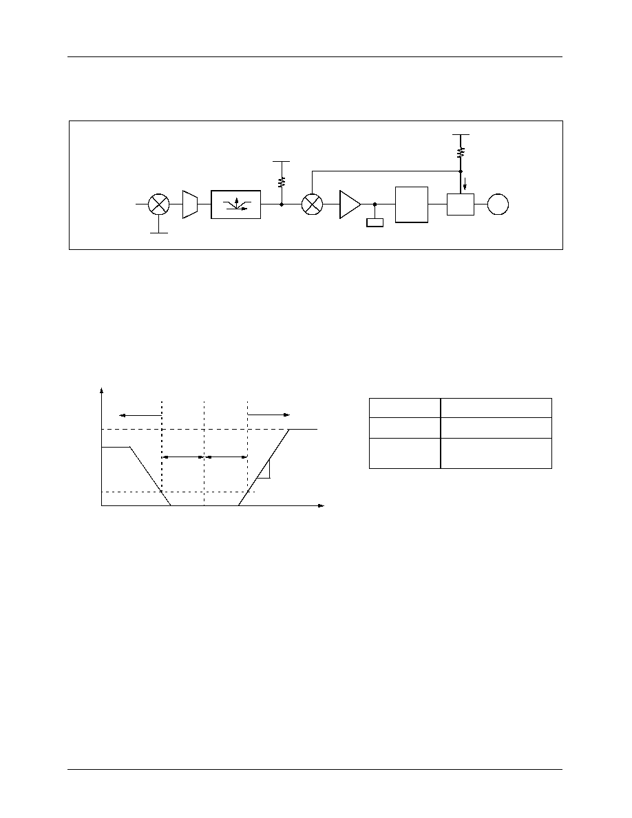
7. Fg Out
8. Hall Sensor Connection
Forward rotation at E
C
< E
CR
Rotating speed is decreased due to reverse torque at E
C
>E
CR
. (Motor still rotates forward)
At the moment that the motor rotates in reverse, the reverse rotation preventer makes the output power transistor open.
Rotating reverse at short time due to motor inertia
Stop within 1/6 turn reverse rotating
H1
-
H1+
H2
-
H2+
H3
-
H3+
FG1X
FG3X
24
19
V
CC
HALL 1
HALL 2
HALL 3
15 VH
V
CC
HALL 1
HALL 2
HALL 3
15 VH

FAN8420D3
13
Rev. 1.0.1
Oct. 2000.
9. Connect A By-pass Capacitor, 0.1
µ
µ
µ
µ
f Between The Supply Voltage Source
(1) the heat radiation fin is connected to the internal gnd of the package.
connect that fin to the external gnd.
25
Vcc
0.1
µ
F
FAN8420D3
14
Rev. 1.0.1
Oct.. 2000.
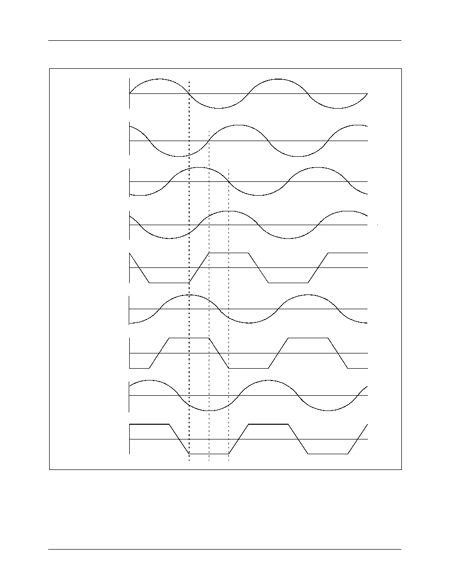
10. Input-output Timing Chart
H1 +
H2 +
H3 +
A1 output current
(H1
-
)+(H2 +)
A3 output current
(H3
-
)+(H1 +)
A3 output voltage
A2 output voltage
A2 output current
(H2
-
)+(H3 +)
A1 output voltage
FAN8420D3
15
Rev. 1.0.1
Oct. 2000.
Test Circuits
1
2
3
4
5
6
7
8
9
10
11
12
13
14
15
16
17
18
19
20
21
22
23
24
25
26
27
28
FAN8420D3
V
V
V
V
V
A
A
A
A
A
A
A
A
A
A
V
V
12V
IM3
VM7
R
CS
0.5
IM2
5V
VR1
10
µ
A
15
VM6
VR2
IM1
VR3
IM2
VR5
0.1
µ
F
VM4
10
µ
A
14
VM5
20mA
13
VM3
IM4
VR9
IM5
IM6
IM7
IM8
IM9
VR10 VR11 VR12 VR13
SW3
a
b
c
SW2
a
b
c
SW1
a
b
c
VM8
VR8
RL=5
RL=5
RL=5
SW13
a
b
VM1
12V
300mA
VM2
300mA
V
10
µ
A
15
VM6
NC
A3
NC
A2
NC
NC
A1
GND
H1+
H1
-
H2+
H2
-
H3+
H3
-
VH
NC
PC1
SB
FG3X
DIR
ECR
EC
SS
FG1X
VCC
NC
VM
CS1
V
FAN8420D3
16
Rev. 1.0.1
Oct.. 2000.
Typical Application Circuits
1
2
3
4
5
6
7
8
9
10
11
12
13
14
19
18
17
16
15
22
21
20
23
24
25
26
27
28
HALL 1
HALL 3
Servo
Signal
ST
HALL 2
1.675V
SP
V
CC
(5V)
V
M
(12V)
FAN8420D3
0.5
R2
R1
0.1
µ
F
NC
A3
NC
A2
NC
NC
A1
GND
H1+
H1
-
H2+
H2
-
H3+
H3
-
CS1
VM
NC
VCC
FG1X
SS
EC
ECR
DIR
FG3X
SB
PC1
NC
VH

FAN8420D3
17
Rev. 1.0.1
Oct. 2000.

FAN8420D3
12/1/00 0.0m 001
Stock#DSxxxxxxxx
2000 Fairchild Semiconductor International
LIFE SUPPORT POLICY
FAIRCHILD'S PRODUCTS ARE NOT AUTHORIZED FOR USE AS CRITICAL COMPONENTS IN LIFE SUPPORT DEVICES
OR SYSTEMS WITHOUT THE EXPRESS WRITTEN APPROVAL OF THE PRESIDENT OF FAIRCHILD SEMICONDUCTOR
INTERNATIONAL. As used herein:
1. Life support devices or systems are devices or systems
which, (a) are intended for surgical implant into the body,
or (b) support or sustain life, and (c) whose failure to
perform when properly used in accordance with
instructions for use provided in the labeling, can be
reasonably expected to result in a significant injury of the
user.
2. A critical component in any component of a life support
device or system whose failure to perform can be
reasonably expected to cause the failure of the life support
device or system, or to affect its safety or effectiveness.
www.fairchildsemi.com
DISCLAIMER
FAIRCHILD SEMICONDUCTOR RESERVES THE RIGHT TO MAKE CHANGES WITHOUT FURTHER NOTICE TO ANY
PRODUCTS HEREIN TO IMPROVE RELIABILITY, FUNCTION OR DESIGN. FAIRCHILD DOES NOT ASSUME ANY
LIABILITY ARISING OUT OF THE APPLICATION OR USE OF ANY PRODUCT OR CIRCUIT DESCRIBED HEREIN; NEITHER
DOES IT CONVEY ANY LICENSE UNDER ITS PATENT RIGHTS, NOR THE RIGHTS OF OTHERS.