 | –≠–ª–µ–∫—Ç—Ä–æ–Ω–Ω—ã–π –∫–æ–º–ø–æ–Ω–µ–Ω—Ç: FAN8727 | –°–∫–∞—á–∞—Ç—å:  PDF PDF  ZIP ZIP |

©2002 Fairchild Semiconductor Corporation
www.fairchildsemi.com
Rev. 1.0.2
Features
∑ Built-in Power Save Circuit
∑ Built-in Current Limit Circuit
∑ Built-in Thermal Shutdown Circuit (TSD)
∑ Built-in Hall Bias
∑ Built-in FG Signal Output Circuit
∑ Built-in Rotational Direction Detecting Circuit
∑ Built-in Protection Circuit For Reverse Rotation
∑ Built-in Short Brake Circuit
∑ Built-in Normal OP-AMP
∑ Built-in 4-CH Balanced Transformerless (BTL) Driver
∑ Built-in BTL MUTE Circuit (CH1-2, CH3 and CH4)
∑ Corresponds to 3.3V DSP
Description
The FAN8727 is a monolithic integrated circuit suitable for a
4-CH motor driver which drives the tracking actuator, focus
actuator, sled motor, loading motor and 3-phase BLDC
spindle motor of the MDP/CAR-MD/CAR-NAVIGATION
system.
48-QFPH-1414
Typical Applications
∑ Mini Disk Player
∑ Digital Video Disk Player
∑ Car Mini Disk Player
∑ Car Navigation System
Ordering Information
Device
Package
Operating Temperature
FAN8727 48-QFPH-1414
-35
∞
C ~ +85
∞
C
FAN8727
Spindle + 4-CH Motor Drive IC

FAN8727
2
Pin Assignments
1
2
3
4
5
6
7
8
9
27
26
25
13
14
15
16
17
18
19
20
21
22
23
24
48
47
46
45
44
43
42
41
40
39
38
37
30
29
28
33
32
31
36
35
34
FAN8727
VH
FG
ECR
EC
VCC2
PC1
SIGGND
VM
CS1
SS
DIR
SB
10
11
12
DO4 +
DO4
-
AVM3
DO3 +
DO3
-
BTLPGND2
BTLPGND1
DO2 +
DO2
-
DO1 +
DO1
-
DI1
H3 +
H3
-
H2 +
H2
-
H1 +
H1
-
BTLS
NGD
BI
AS
AV
M
4
MUTE12
MUTE3
MUTE4
PWRGND
A3
A2
A1
OP
I
N
+
OP
I
N
-
OPOUT
VCC
1
AV
M
1
2
DI
4
DI
3
DI
2

FAN8727
3
Pin Definitions
Pin Number
Pin Name
I/O
Pin Function Description
1
VH
I
Hall Bias
2
FG
O
FG Signal Output
3
ECR
I
Torque Control Reference
4
EC
I
Torque Control Signal
5
VCC2
-
Supply Voltage
6
PC1
-
Phase Compensation Capacitor
7
SIGGND
-
Signal Ground
8
VM
-
Motor Supply Voltage
9
CS1
I
Current Sensor
10
S/S
I
Start/stop
11
DIR
O
3-Phase Rotational Direction Output
12
SB
I
Short Brake
13
PWRGND
-
Power Ground
14
A3
O
3-Phase Output 3
15
A2
O
3-Phase Output 2
16
A1
O
3-Phase Output 1
17
OPIN+
I
OP-AMP Input (+)
18
OPIN-
I
OP-AMP Input (-)
19
OPOUT
O
OP-AMP Output
20
VCC1
-
Supply Voltage
21
AVM12
-
BTL CH1, 2 Motor Supply Voltage
22
DI4
I
BTL Drive Input 4
23
DI3
I
BTL Drive Input 3
24
DI2
I
BTL Drive Input 2
25
DI1
I
BTL Drive Input 1
26
DO1-
O
BTL Drive 1 Output (-)
27
DO1+
O
BTL Drive 1 Output (+)
28
DO2-
O
BTL Drive 2 Output (-)
29
DO2+
O
BTL Drive 2 Output (+)
30
BTLPGND1
-
BTL Power Ground 1
31
BTLPGND2
-
BTL Power Ground 2
32
DO3-
O
BTL Drive 3 Output (-)
33
DO3+
O
BTL Drive 3 Output (+)

FAN8727
4
Pin Definitions
(Continued)
Pin Number
Pin Name
I/O
Pin Function Description
34
AVM3
-
BTL CH3 Motor Supply Voltage
35
DO4-
O
BTL Drive 4 Output (-)
36
DO4+
O
BTL Drive 4 Output (+)
37
MUTE4
I
BTL Drive Mute CH4
38
MUTE3
I
BTL Drive Mute CH3
39
MUTE12
I
BTL Drive Mute CH1, 2
40
AVM4
-
BTL CH4 Motor Supply Voltage
41
BIAS
-
BTL Bias Voltage
42
BTLSGND
-
BTL Drive Signal Ground
43
H1-
I
Hall1(-) Input
44
H1+
I
Hall1(+) Input
45
H2-
I
Hall2(-) Input
46
H2+
I
Hall2(+) Input
47
H3-
I
Hall3(-) Input
48
H3+
I
Hall3(+) Input
FAN8727
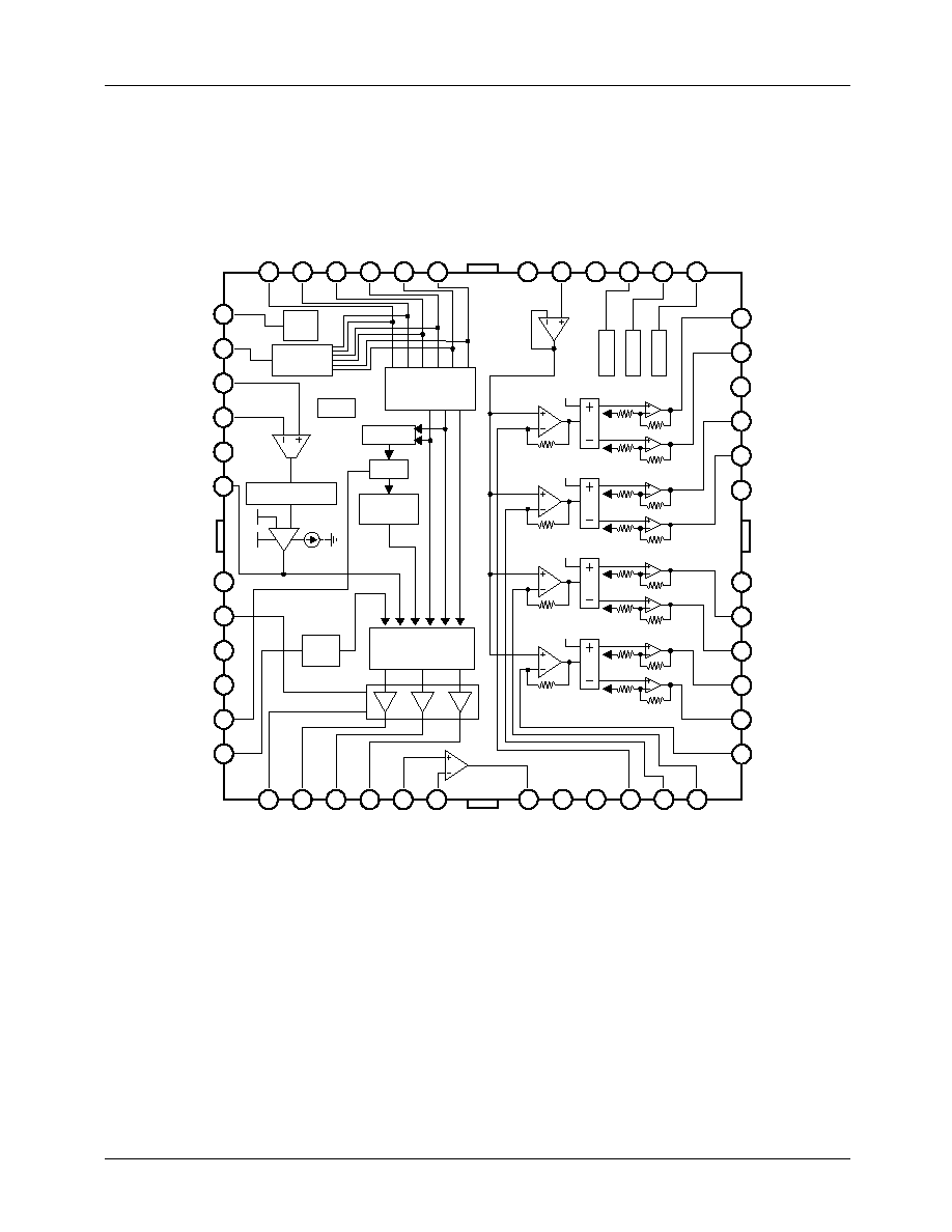
5
Internal Block Diagram
FG
VH
ECR
EC
VCC2
PC1
SB
SIGGND
VM
CS1
SS
DIR
A2
OPIN-
PWRGND
A1
OPIN+
A3
VCC1
OPOUT
DI2
DI4
AVM12
DI3
DO4-
DO3+
DO3-
DO4+
BTLPGND2
AVM3
BTLPGND1
DO2+
DO1-
DO2-
DO1+
DI1
H1-
H1+
H2+
H2-
H3+
H3-
MUTE4
AVM4
MUTE12
BTLSGND
BIAS
MUTE3
Hall Amp
MUTE12
MUTE3
MUTE4
Distributor
Logic
Detection
Reverse
Rotation
Short
Brake
FG
Generator
Hall
Bias
6
5
4
3
2
1
12
11
10
9
8
7
18
17
16
15
14
13
24
22
23
21
20
19
30
29
28
27
26
25
36
35
34
33
32
31
37
38
39
40
41
42
48
47
46
45
44
43
AVM4
AVM3
AVM12
AVM12
TSD
Absolute Values
Current
Sense Amp
Output
Current Limit
CS1
VM

FAN8727
6
Equivalent Circuits
Hall Bias
FG Signal Output
Torque Control Reference & Signal
Phase Compensation Capacitor
Current Detector
Start/Stop
100K
1
2
25
10K
3
25
4
1K
25
6
1K
9
5K
10
25
50K
30K
100K

FAN8727
7
Equivalent Circuits
(Continued)
3-Phase Rotational Direction Output
Short Brake
3-Phase Output
OP-AMP Input
OP-AMP Ouput
BTL Drive Input
11
25
10K
12
25
1k
20k
14
15
16
15K
17
25
1K
2K
25
1K
2K
18
2K
2K
18
23
24
25
25
50
22

FAN8727
8
Equivalent Circuits
(Continued)
BTL Drive Output
BTL Drive Mute
BTL Bias Voltage
Hall Input
27
28
29
26
33
35
36
32
30K
20K
38
39
25
50K
37
30K
41
25
0.5K
45
25
1K
47
43
46
25
1K
48
44
FAN8727
9
Absolute Maximum Ratings ( Ta=25
∞
∞
∞
∞
C)
Note:
1.
When mounted on 70mm
◊
70 mm
◊
1.6mm PCB (Phenolic resin material)
2.
Power dissipation is reduced 24 mW/
∞
C for using above Ta=25
∞
C
3.
Do not exceed Pd and SOA.
Recommended Operating Conditions ( Ta=25
∞
∞
∞
∞
C)
Note: The VM should be turn on before the VCC2.
Parameter
Symbol
Value
Unit
Supply Voltage (BTL Signal)
Supply Voltage (Spindle Signal)
Supply Voltage (Motor)
Supply Voltage (BTL Motor)
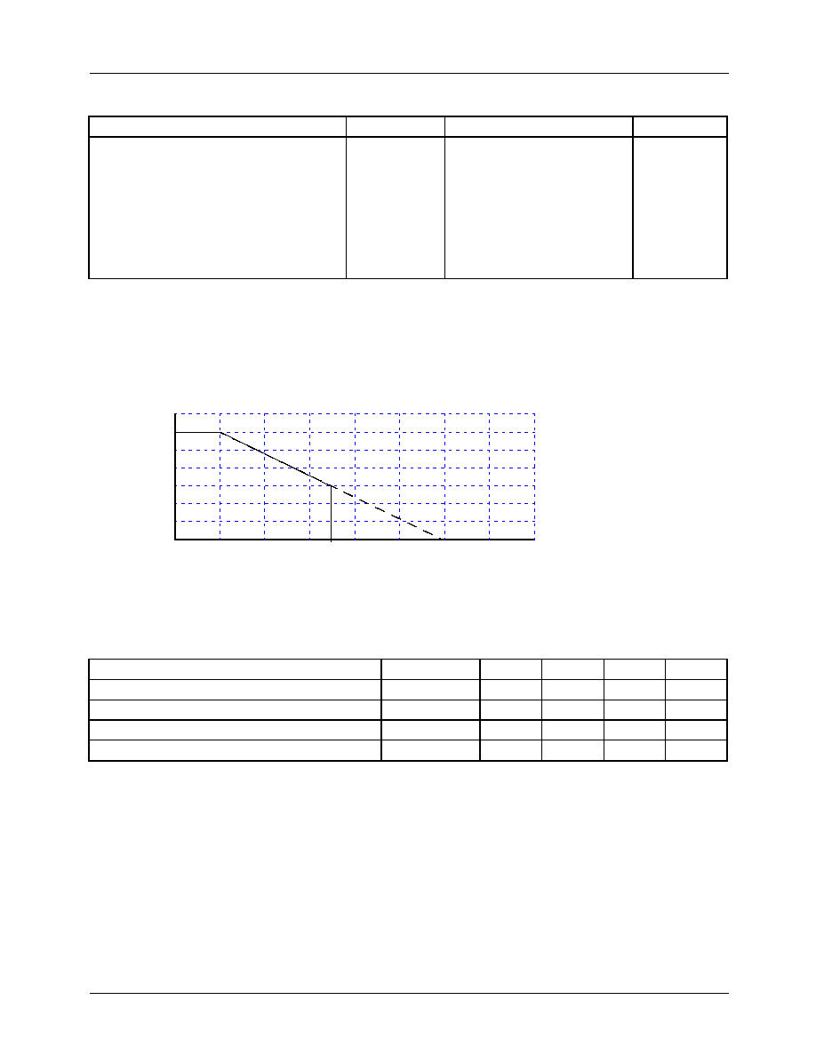
Power Dissipation
Operating Temperature Range
Storge Temperature Range
Maximum Output Current (Spindle Part)
Maximum Output Current (BTL Part)
V
CC1max
V
CC2max
V
Mmax
V
MBTLmax
Pd
Topr
Tstg
I
OMAXS
I
OMAXB
15
7
15
15
3.0
note
-35 ~ +85
-55 ~ +150
1.3
1
V
V
V
V
W
∞
∞
∞
∞
C
∞
∞
∞
∞
C
A
A
Parameter
Symbol
Min.
Typ.
Max.
Unit
Operating Supply Voltage (BTL Signal)
V
CC1
4.5
-
13.2
V
Operating Supply Voltage (Spindle Signal)
V
CC2
4.5
-
5.5
V
Operating Supply Voltage ( Spindle Motor)
V
M
note
4.5
-
13.2
V
Operating Supply Voltage (BTL Motor)
V
MBTL
4.5
-
V
CC1
V
175
150
125
100
75
50
25
0
1,000
2,000
3,000
Pd [mW]
Ambient Temperature, Ta [
∞
C]
0

FAN8727
10
Electrical Characteristics
(Ta=25
∞
C, V
CC2
=5V, V
M
=12V)
Note: Guaranteed field ( No EDS / Final test )
Parameter
Symbol
Condition
Min.
Typ.
Max.
Unit
Circuit Current 1
I
CC 1
Power Save=0V
-
0.3
1
mA
Circuit Current 2
I
CC2
Power Save=5V
-
4.5
6
mA
START/STOP
On Voltage Range
V
PSON
L-H Circuit On
2.5
-
-
V
Off Voltage Range
V
PSOFF
H-L Circuit Off
-
-
0.5
V
HALL BIAS
Hall Bias Voltage
V
HB
I
HB
= 20mA
-
1.2
1.8
V
HALL AMP
Hall Bias Current
I
HA
-
-
1
5
uA
In-Phase in Voltage Range
V
HAR
-
1.5
-
4.0
V
Minimum in Level
note
V
INH
-
60
-
-
mVpp
TORQUE CONTROL
In Voltage Range
E
C
-
0.5
-
3.3
V
Offset Voltage (-)
note
E
COFF-
E
CR
= 2.5V
-100
-50
-20
mV
Offset Voltage (+)
E
COFF+
E
CR
= 2.5V
20
50
100
mV
In Current
E
CIN
E
C
= E
CR
= 2.5V
-5
-1
-
uA
In/Output Gain
G
EC
E
CR
= 2.5V, R
CS
= 0.5
0.41
0.51
0.61
A / V
FG
FG Output Voltage (H)
V
FGH
I
FG
= -10uA
3.0
-
V
CC
V
FG Output Voltage (L)
V
FHL
I
FG
= 10uA
-
-
0.5
V
Input Voltage Range
note
V
FGR
Hn+, Hn- input D-range
1.5
-
4.0
V
OUTPUT BLOCK
Saturation Voltage (Upper TR)
V
OH
I
O
= -300mA
-
0.9
1.6
V
Saturation Voltage (Lower TR)
V
OL
I
O
= 300mA
-
0.2
0.6
V
Torque Limit Current
I
TL
R
CS
= 0.5
560
700
840
mA
DIRECTION DETECTOR
Dir Output Voltage (H)
V
DIRH
I
FG
= -10uA
3.0
-
V
CC
V
Dir Output Voltage (L)
V
DIRL
I
FG
= 10uA
-
-
0.5
V
SHORT BRAKE
On Voltage Range
V
SBON
-
2.5
-
V
CC
V
Off Voltage Range
V
SBOFF
-
0
-
1.0
V

FAN8727
11
Electrical Characteristics
(Continued)
BTL Drive Part (Ta=25
∞
C, V
CC1
=12V, V
MBTL
=12V, R
L
=24
)
Note: Guaranteed field ( No EDS / Final test )
Parameter
Symbol
Condition
Min.
Typ.
Max.
Unit
Quiescent Circuit Current
I
CC
-
-
18
25
mA
Output Offset Voltage
V
OO
-
-40
-
40
mV
Maximum Output
Amplitude Voltage
V
OM
-
9.5
10.5
-
V
Voltage Gain
G
VC
V
IN
=0.1Vrms, 1kHz
10.5
12.0
13.5
dB
Ripple Rejection Ratio
note
RR
V
IN
=0.1Vrms, 120kHz
-
60
-
dB
Slew Rate
note
SR
120Hz, 2Vpp
-
1.0
-
V/us
CH Mute off Voltage
V
MOFFCH
Pin37, 38, 39 = Variation
-
-
1.0
V
CH Mute On Voltage
V
MONCH
Pin37, 38, 39 = Variation
2.5
-
-
V
NORMAL OP- AMP
Input Offset Voltage
V
OF
-
-20
-
+20
mV
Input Bias Current
I
B1
-
-
-
600
nA
High Level Output Voltage
V
OH1
-
11
-
-
V
Low Level Output Voltage
V
OL1
-
-
-
0.1
V
Output Sink Current
I
SINK
-
10
25
-
mA
Output Source Current
I
SOU1
-
5
8
-
mA
Open Loop Voltage Gain
note
G
VO1
f=1kHz, V
IN
= -75dB
-
75
-
dB
Ripple Rejection Ratio
note
RR1
f=120Hz, V
IN
= -20dB
-
65
-
dB
Slew Rate
note
SR1
f=120Hz, 2Vp-p
-
1
-
V/us
Common Mode Rejection Ratio
note
CMRR1
f=1kHz, V
IN
= -20dB
-
80
-
dB

FAN8727
12
Calculation of Gain & Torque Limit Current
0.255 which is made from GM times R1 is fixed value within IC.
Vmax (see above block diagram) is setted to 350mV.
EC
ECR
+
-
Gm
-
+
+
Absolute
Values
Current / Voltage
Convertor
R1
Vin
+
-
Driver
VM
Vmax
Max. output current limiting
+
-
VM
VM
Negative
Feedback loop
I
O
R
S
V
S
-
+
CS1 (Pin 9)
Output
Current sense
Power
Transistors
Commutation
Distributor
U
V
W
H1
H2
H3
I
O
Gain
0.255
R
S
---------------
=
Itl mA
[
]
Vmax
R
S
----------------
350 mV
[
]
R
S
------------------------
=
=

FAN8727
13
Application Information
1. Mute Function
1) Mute Control Voltage Condition
When using the mute function, the applied control voltage condition is as follows.
2) Separated Channel Mute Function
These pins are used for individual channel mute operation.
- When the mute pins (pin 37, 38 and 39) are OPEN or the voltage of the mute pins are below 0.5[V], the mute circuit is
stopped and BTL output circuits operate normally.
- When the mute pins (pin 37, 38 and 39) are above 2.5[V], the mute circuits are activated so that the BTL output circuits
will be muted.
- If the junction temperature rises above 175
∞
C, then the thermal shutdown (TSD) circuit is activated and all the output
circuits (4-CH BTL Drivers and 3-phase BLDC Driver) are muted.
2. 4-CH Balanced Transformerless (Btl) Driver
- The voltage, Vbias, is the reference voltage given by the external bias voltage of pin 41.
- The input signals, Vin, through the pins (pin 22, 23, 24 and 25) are amplified 10K/Rextern times and then fed to the level
shift.
- The level shift produces the current due to the difference between the input signal (Vin) and the arbitrary reference
voltage (Vbias). The current produced as +
I and -
I are fed into the drive buffers.
- The drive buffer operates the power TR of the output stage according to the state of the input signal(Vin).
- The output stage is the BTL driver, and the motor (or actuator) is rotating in forward direction by operating TR Q1 and
TR Q4. On the other hand, if TR Q2 and TR Q3 are operating, the motor (or actuator) is rotating in reverse direction.
- When the input signal Vin, through the pin (pin 22, 23, 24 and 25) is below the Vbias, then the motor (actuator) is in
forward direction.
MUTE ON Voltage
2.5[V] Above
Mute Function Operation
MUTE OFF
Voltage
OPEN or 0.5[V] Below
Normal Operation
+
-
VCC
Q1
Q2
Q3
Q4
LEVEL
SHIFT
AMP1
GND
DRIVE
AMP
DRIVE
AMP
M
41
22 23
24 25
27
29
33
36
26
28
32
35
Rextern
10k
Vbias
Vin
X2
X2

FAN8727
14
- When the input signal Vin, through the pin (pin 22, 23, 24 and 25) is above the Vbias, then the motor (actuator) is in
reverse direction.
- If you want to change the gain, then modify the external resistor's value (Rextern)
3. Torque & Output Current Control
Torque Control & Output Current Control
- By amplifying the voltage difference between E
C
and E
CR
from the Servo IC, the torque sense AMP produces the input
(V
AMP
) for the current sense AMP.
- The current sense AMP produces the input for the Gain controller to allow the output current (I
O
) of the driver to be
controlled by the input voltage (V
AMP
), where the output current (I
O
) is detected by the sense resistor (R
NF
) and is
converted into V
RNF
.
- In the end, the signals of the Servo IC control the velocity of the motor by controlling the output current (I
O
) of the
driver.
- When the junction temperature rises up to about 175
∞
C, then the output drive circuit will be shut down.
- The range of the torque control input voltage is as shown below.
The input range (E
C
) of the Torque Sense AMP is 0.5V ~ 3.3V
+
-
+
-
Torque sense amp
E
CR
E
C
Current sense amp
TSD
Gain
Controller
Driver
M
R
NF
I
O
V
M
V
AMP
V
RNF
+
-
V
M
Forward
Ecoff+
Ecoff
-
Reverse
V
RNF
[V]
3 mV
0
E
CR
-E
C
[V]
Rotation
Ec < E
CR
Forward rotation
Ec > E
CR
Stop after detecting
reverse rotation
FAN8727
15
4. Power Save Function
- This function block operates the power saving function.
- The power save circuit is activated by operating TR Q1.
- When the SS (Start/Stop) pin 10 is high (V
CC
), the TR Q1 is turned on so that the bias circuit is enabled. On the other
hand, when the SS (Start/Stop) pin 10 is Open or Low (GND), the TR Q1 is turned off so that the bias circuit is disabled.
- The power save operation controlled by SS (pin 10) input conditions is as follows;
5. Short Brake Function
When the pick-up part moves from the inner to the outer spindle of the MD, the brake function of the reverse voltage is com-
monly employed to rate the rotational velocity of the spindle motor.However, if the spindle motor rotates rapidly, the brake
function of the reverse voltage may produce too much heat at the drive IC.
To remove these shortcomings and to enhance efficiency, the short brake function is added to FAN8727. When the short brake
function is active, all upper Power transistors are turned off and the lower Power transistors turned on, so as to reduce the rota-
tional velocity of the motor. The short brake operation controlled by SB (pin 12), and the inputs conditions are as follows.
Pin#10
FAN8727
HIGH
START
OPEN/LOW
STOP
Pin#12
SHORT BRAKE
HIGH
ON
LOW
OFF
10
V
CC
Start
Stop
12K
30K
Q1
100k
Bias block
14
15
16
MOTOR
OFF
ON
12
V
CC
ON
OFF
80K
1K
Q1
Drive logic
V
M

FAN8727
16
6. Thermal Shutdown (Tsd) Function
When the junction temperature rises up to about 175
∞
C, then the output drive circuit is shut down, when the junction tempera-
ture falls off to about 160
∞
C, the output drive circuit will be normally operated. It has the temperature hysteresis of about 15
∞
C.
7. Rotational Direction Detecting Function
- The forward and reverse rotations of the MD are detected by the circuit, as shown in the above Table.
- The rotational direction of the MD can be learned by the output waveforms of the hall sensor and/or the driver. Let the
three hall sensors be H1, H2 and H3 respectively. If the hall sensors turn on in the order, H1
H2
H3, of the reverse
rotation, the output waveforms of the hall sensors will be as shown below.
Inversely, if the hall sensors turn on in the order, H3
H2
H1, of the forward rotation, the output waveforms of the hall sen-
sors will be as shown mext page.
11
+
-
+
-
V
CC
DIR
D-F/F
D
Q
CK
H2+
H3+
H3
-
H2
-
Rotation
DIR
E
C
< E
CR
Forward
Low
E
C
> E
CR
Reverse
High
R
( a)
H1
H2
H3

FAN8727
17
In the cases above, the value of H2 at the falling edges of H3 is Low in figure <a>, while High in figure <b>. The rotational
direction detector takes advantage of this phenomenon.
8. Reverse Rotation Preventing Function
- The forward and reverse rotation of the motor are detected, as shown in the table below, by the circuit shown above.
Consequently at reverse rotation, the D-F/F output Q becomes Low and cuts off the output current sense Amp, resulting
in the stoppage of the Gain controller function.
- When the MD is rotating in forward direction, E
C
>E
CR
is sometimes controlled to retard and/or stop the MD. As the
controlling time of E
C
>E
CR
gets longer, MD slows down, stops, and then rotates in the reverse direction. To prevent the
MD from rotating in the reverse direction, a reverse rotation resistant function is required. Its operational principles are
discussed below.
Rotation
H2
H3
D-F/F
Reverse Rotation Preventer
E
C
<E
CR
E
C
>E
CR
Forward
H H
L
H
Forward
Brake and Stop
Reverse
L
H
L
L
-
Stop
( b)
H1
H2
H3
+
-
+
-
+
-
Current
Sense
Amp
Gain
Controller
Driver
D-F/F
M
D
Q
CK
H3+
H3
-
H2+
H2
-
E
C
E
CR

FAN8727
18
9. FG Output Function
The FG output, which detects the number of rotations of the MD, is generated by combination zero-crossing the output wave-
forms of the hall sensors. The FG output circuit is as shown below.
10. Hall Sensor Connection
External Hall sensors are used in series or parallel connection as shown below.
+
-
+
-
+
-
H1
H2
H3
FG OUTPUT
V
CC
HALL 1
HALL 2
HALL 3
1 VH
V
CC
HALL 1
HALL 2
HALL 3
1 VH

FAN8727
19
11. Hall Input Output Timming Chart
The 3-phase hall signal is amplified in the hall amplifiers and sent to the matrix section, where the signal is further amplified
and combined. After the signal is converted to a current in the amplitude control circuit, the current is supplied to the output
driver, which then provides a motor drive current. The phases of the hall input signal, output voltage, and output current are
shown below.
H1 +
H2 +
H3 +
A1 output current
A3 output current
A3 output voltage
A2 output voltage
A2 output current
A1 output voltage

FAN8727
20
Test Circuits 1
BTL Drive Part
1
2
3
4
5
6
7
8
9
10
11
12
43
44
45
46
47
48
FAN8727
25
26
27
28
30
29
31
32
33
34
35
36
37
38
39
40
41
42
12V
10
µ
F
2.5V
VMUTE
VMUTE
VMUTE
RL4'
RL4
RL3'
RL3
SW4
SW3
RL2
V
V
V
V
SW2
SW1
RL1
SERVO AMP
TRACKING
FOCUS
SLED
CONTROL TRAY
12V
10
µ
F
10
µ
F
12V
BTL SVCC
A
12V
10
µ
F
13
14
15
16
17
19
22
18
20
21
24
23
V
V
V
V
OPIN (+)
OPIN (
-
)
OPOUT
SW5
1
2
3
1M
V
IN1
V
p1
1.2k
V
CC
SW7
1
2
3
SW6
V
IN3
V
s1
10
µ
F
1M
2
3
1
V
IN3
+
-
VH
FG
ECR
EC
VCC2
PC1
SIGGND
VM
CS1
SS
DIR
SB
DO4+
DO4
-
AVM3
DO3+
DO3
-
BTLPGND2
BTLPGND1
DO2+
DO2
-
DO1+
DO1
-
DI1
H3+
H3
-
H2+
H2
-
H1+
H1
-
BTLSGND
BI
AS
AV
M
4
MUTE12
MUTE3
MUTE4
PWRGND
A3
A2
A1
OPI
N
-
OPI
N
+
OPOUT
VCC1
AV
M
1
2
D14
D13
D12

FAN8727
21
Test Circuits 2
Spindle Motor Drive Part
1
2
3
4
5
6
7
8
9
10
11
12
13
14
15
16
17
19
20
21
22
23
24
25
26
27
28
30
29
31
32
33
34
35
36
37
38
39
40
42
41
43
44
45
46
47
48
FAN8727
18
A
A
A
A
A
A
V
V
A
V
V
H3+ H3
-
H2+ H2
-
H1+ H1
-
SW12
SW13
SW14
2.5V
5V
12V
SW15
SW16
SW17
SW18
IFR
SW19 SW20
VSB
E
C
VH
FG
ECR
EC
VCC2
PC1
SIGGND
VM
CS1
SS
DIR
SB
DO4+
DO4
-
AVM3
DO3+
DO3
-
BTLPGND2
BTLPGND1
DO2+
DO2
-
DO1+
DO1
-
DI1
H3+
H3
-
H2+
H2
-
H1+
H1
-
BTL
S
GND
BI
AS
AV
M
4
MUTE1
2
MUT
E
3
MUT
E
4
PW
RGND
A3
A2
A1
OP
I
N
-
OP
I
N
+
OP
O
U
T
VCC1
AV
M
1
2
D14
D13
D12

FAN8727
22
Application Circuits
42
FAN8727
1
2
3
4
5
6
7
8
9
10
11
12
13
14
15
16
17
18
19
20
21
22
23
24
25
26
27
28
29
30
31
32
33
34
35
36
37
38
39
40
41
43
44
45
46
47
48
HAL
L
3
HAL
L
2
HAL
L
1
BT
L B
I
AS
VOL
T
AGE
+5V
F
O
C
U
S TR
ACKI
NG
MUTE
SL
ED MUT
E
TR
A
Y
M
U
TE
TRAY
MOTOR
+5V
SLED
MOTOR
FOCUS
ACTUATOR
TRACKING
ACTUATOR
SERVO AMP
TRACKING
FOCUS
SLED
CONTROL TRAY
+5V
VCC
SHORT
BREAK
ROTATE
DIRECTION
SYSTEM
CONTROL
12V
0.1
µ
F
VCC
SERVO
TORQUE
CONTROL
FG SIGNAL
VH
FG
ECR
EC
VCC2
PC1
SIGGND
VM
CS1
SS
DIR
SB
DO4+
DO4
-
AVM3
DO3+
DO3
-
BTLPGND2
BTLPGND1
DO2+
DO2
-
DO1+
DO1
-
DI1
H3+
H3
-
H2+
H2
-
H1+
H1
-
BT
LSGND
BI
AS
AV
M
4
MUTE1
2
MUT
E
3
MUT
E
4
PWRGND
A3
A2
A1
OPI
N
-
OPI
N
+
OPOUT
VCC1
AV
M
1
2
D14
D13
D12
100pF
10K

FAN8727
23

FAN8727
9/6/02 0.0m 001
Stock#DSxxxxxxxx
2002 Fairchild Semiconductor Corporation
LIFE SUPPORT POLICY
FAIRCHILD'S PRODUCTS ARE NOT AUTHORIZED FOR USE AS CRITICAL COMPONENTS IN LIFE SUPPORT DEVICES
OR SYSTEMS WITHOUT THE EXPRESS WRITTEN APPROVAL OF THE PRESIDENT OF FAIRCHILD SEMICONDUCTOR
CORPOTATION. As used herein:
1. Life support devices or systems are devices or systems
which, (a) are intended for surgical implant into the body,
or (b) support or sustain life, and (c) whose failure to
perform when properly used in accordance with
instructions for use provided in the labeling, can be
reasonably expected to result in a significant injury of the
user.
2. A critical component in any component of a life support
device or system whose failure to perform can be
reasonably expected to cause the failure of the life support
device or system, or to affect its safety or effectiveness.
www.fairchildsemi.com
DISCLAIMER
FAIRCHILD SEMICONDUCTOR RESERVES THE RIGHT TO MAKE CHANGES WITHOUT FURTHER NOTICE TO ANY
PRODUCTS HEREIN TO IMPROVE RELIABILITY, FUNCTION OR DESIGN. FAIRCHILD DOES NOT ASSUME ANY
LIABILITY ARISING OUT OF THE APPLICATION OR USE OF ANY PRODUCT OR CIRCUIT DESCRIBED HEREIN; NEITHER
DOES IT CONVEY ANY LICENSE UNDER ITS PATENT RIGHTS, NOR THE RIGHTS OF OTHERS.