 | ÐлекÑÑоннÑй компоненÑ: FCP11N60 | СкаÑаÑÑ:  PDF PDF  ZIP ZIP |
Äîêóìåíòàöèÿ è îïèñàíèÿ www.docs.chipfind.ru
SuperFET
©2004 Fairchild Semiconductor Corporation
Rev. B, March 2004
FCP11N60
/FCPF11N60
TM
FCP11N60/FCPF11N60
General Description
SuperFET
TM
is a new generation of high voltage MOSFETs
from Fairchild with outstanding low on-resistance and low
gate charge performance, a result of proprietary technology
utilizing advanced charge balance mechanisms.
This advanced technology has been tailored to minimize
conduction loss, provide superior switching performance,
and withstand extreme dv/dt rate and higher avalanche
energy. Consequently, SuperFET is very suitable for
various AC/DC power conversion in switching mode
operation for system miniaturization and higher efficiency.
Features
· 650V @T
j
= 150
°
C
· Typ. Rds(on)=0.32
· Ultra low gate charge (typ. Qg=40nC)
· Low effective output capacitance (typ. Coss.eff=95pF)
· 100% avalanche tested
Absolute Maximum Ratings
T
C
= 25°C unless otherwise noted
* Drain current limited by maximum junction termperature
Thermal Characteristics
Symbol
Parameter
FCP11N60
FCPF11N60
Units
I
D
Drain Current
- Continuous (T
C
= 25°C)
11
11*
A
- Continuous (T
C
= 100°C)
7
7*
A
I
DM
Drain Current
- Pulsed
(Note 1)
33
33*
A
V
GSS
Gate-Source Voltage
±
30
V
E
AS
Single Pulsed Avalanche Energy
(Note 2)
340
mJ
I
AR
Avalanche Current
(Note 1)
11
A
E
AR
Repetitive Avalanche Energy
(Note 1)
12.5
mJ
dv/dt
Peak Diode Recovery dv/dt
(Note 3)
4.5
V/ns
P
D
Power Dissipation (T
C
= 25°C)
125
36
W
- Derate above 25°C
1.0
0.29
W/°C
T
J
, T
STG
Operating and Storage Temperature Range
-55 to +150
°C
T
L
Maximum lead temperature for soldering purposes,
1/8
"
from case for 5 seconds
300
°C
Symbol
Parameter
FCP11N60
FCPF11N60
Units
R
JC
Thermal Resistance, Junction-to-Case
1.0
3.5
°C
/
W
R
CS
Thermal Resistance, Case-to-Sink
0.5
--
°C
/
W
R
JA
Thermal Resistance, Junction-to-Ambient
62.5
62.5
°C
/
W
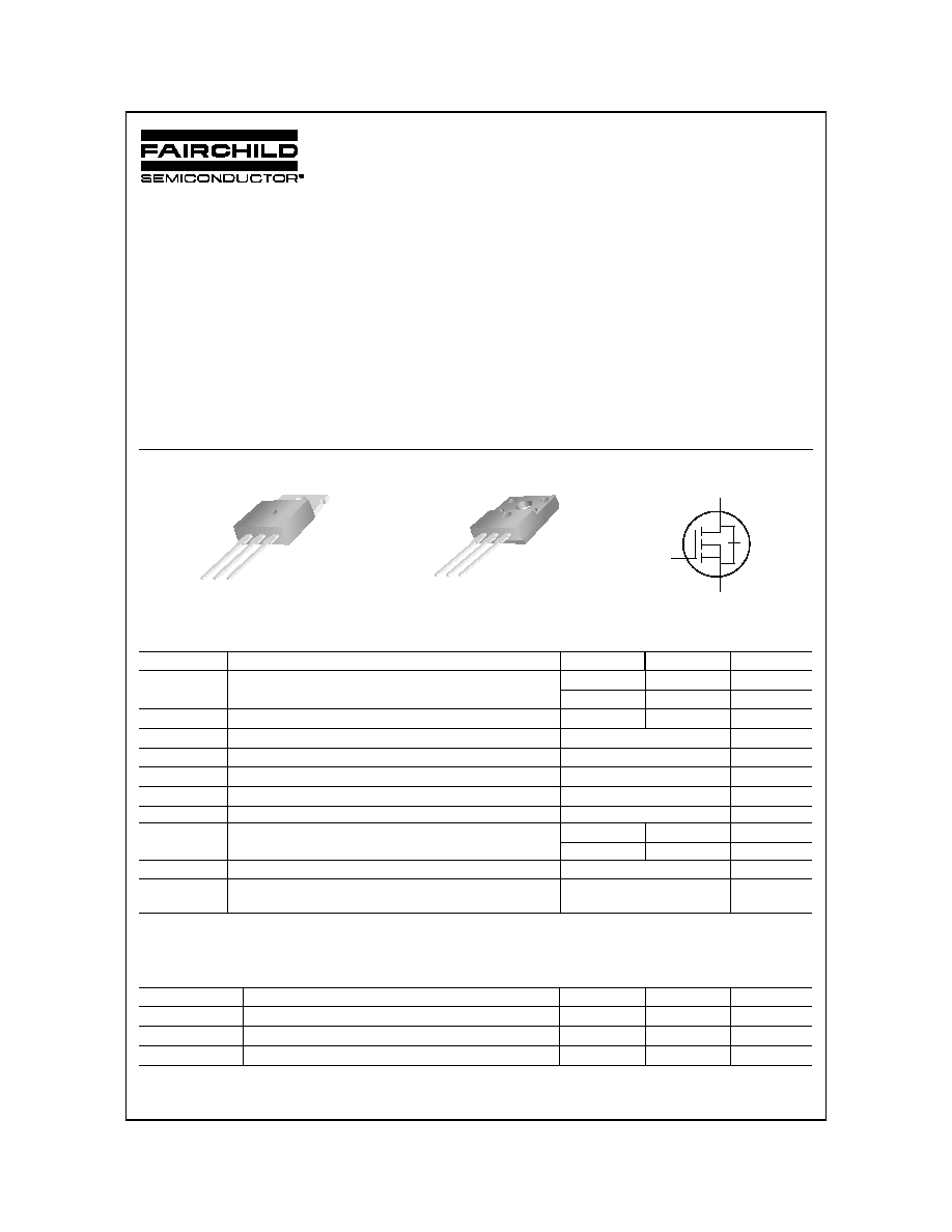
TO-220
FCP Series
G
S
D
TO-220F
FCPF Series
G
S
D
!
!
!
!
!
!
!
!
!
!
!
!
!
!
!
!
!
!
!
!
!
!
!
!
S
D
G
Rev. B, March 2004
FCP11N60
/FCPF11N60
©2004 Fairchild Semiconductor Corporation
Electrical Characteristics
T
C
= 25°C unless otherwise noted
Notes:
1. Repetitive Rating : Pulse width limited by maximum junction temperature
2. I
AS
= 5.5A, V
DD
= 50V, R
G
= 25
,
Starting T
J
= 25°C
3. I
SD
11A, di/dt
200A/
µ
s, V
DD
BV
DSS,
Starting T
J
= 25°C
4. Pulse Test : Pulse width
300
µ
s, Duty cycle
2%
5. Essentially independent of operating temperature
Symbol
Parameter
Test Conditions
Min
Typ
Max
Units
Off Characteristics
BV
DSS
Drain-Source Breakdown Voltage
V
GS
= 0 V, I
D
= 250
µ
A, T
J
= 25°C
600
--
--
V
V
GS
= 0 V, I
D
= 250
µ
A, T
J
= 150°C
--
650
--
V
BV
DSS
/
T
J
Breakdown Voltage Temperature Coef-
ficient
I
D
= 250
µ
A, Referenced to 25°C
--
0.6
--
V/°C
BV
DS
Drain-Source Avalanche Breakdown
Voltage
V
GS
= 0 V, I
D
= 11 A
--
700
--
V
I
DSS
Zero Gate Voltage Drain Current
V
DS
= 600 V, V
GS
= 0 V
--
--
1
µ
A
V
DS
= 480 V, T
C
= 125°C
--
--
10
µ
A
I
GSSF
Gate-Body Leakage Current, Forward
V
GS
= 30 V, V
DS
= 0 V
--
--
100
nA
I
GSSR
Gate-Body Leakage Current, Reverse
V
GS
= -30 V, V
DS
= 0 V
--
--
-100
nA
On Characteristics
V
GS(th)
Gate Threshold Voltage
V
DS
= V
GS
, I
D
= 250
µ
A
3.0
--
5.0
V
R
DS(on)
Static Drain-Source
On-Resistance
V
GS
= 10 V, I
D
= 5.5 A
--
0.32
0.38
g
FS
Forward Transconductance
V
DS
= 40 V, I
D
= 5.5 A
(Note 4)
--
9.7
--
S
Dynamic Characteristics
C
iss
Input Capacitance
V
DS
= 25 V, V
GS
= 0 V,
f = 1.0 MHz
--
1148
1490
pF
C
oss
Output Capacitance
--
671
870
pF
C
rss
Reverse Transfer Capacitance
--
63
82
pF
C
oss
Output Capacitance
V
DS
= 480 V, V
GS
= 0 V,
f = 1.0 MHz
--
35
--
pF
C
oss
eff.
Effective Output Capacitance
V
DS
= 0V to 480 V, V
GS
= 0 V
--
95
--
pF
Switching Characteristics
t
d(on)
Turn-On Delay Time
V
DD
= 300 V, I
D
= 11 A,
R
G
= 25
(Note 4, 5)
--
34
80
ns
t
r
Turn-On Rise Time
--
98
205
ns
t
d(off)
Turn-Off Delay Time
--
119
250
ns
t
f
Turn-Off Fall Time
--
56
120
ns
Q
g
Total Gate Charge
V
DS
= 480 V, I
D
= 11 A,
V
GS
= 10 V
(Note 4, 5)
--
40
52
nC
Q
gs
Gate-Source Charge
--
7.2
--
nC
Q
gd
Gate-Drain Charge
--
21
--
nC
Drain-Source Diode Characteristics and Maximum Ratings
I
S
Maximum Continuous Drain-Source Diode Forward Current
--
--
11
A
I
SM
Maximum Pulsed Drain-Source Diode Forward Current
--
--
33
A
V
SD
Drain-Source Diode Forward Voltage
V
GS
= 0 V, I
S
= 11 A
--
--
1.4
V
t
rr
Reverse Recovery Time
V
GS
= 0 V, I
S
= 11 A,
dI
F
/ dt = 100 A/
µ
s
(Note 4)
--
390
--
ns
Q
rr
Reverse Recovery Charge
--
5.7
--
µ
C
©2004 Fairchild Semiconductor Corporation
Rev. B, March 2004
FCP11N60
/FCPF11N60
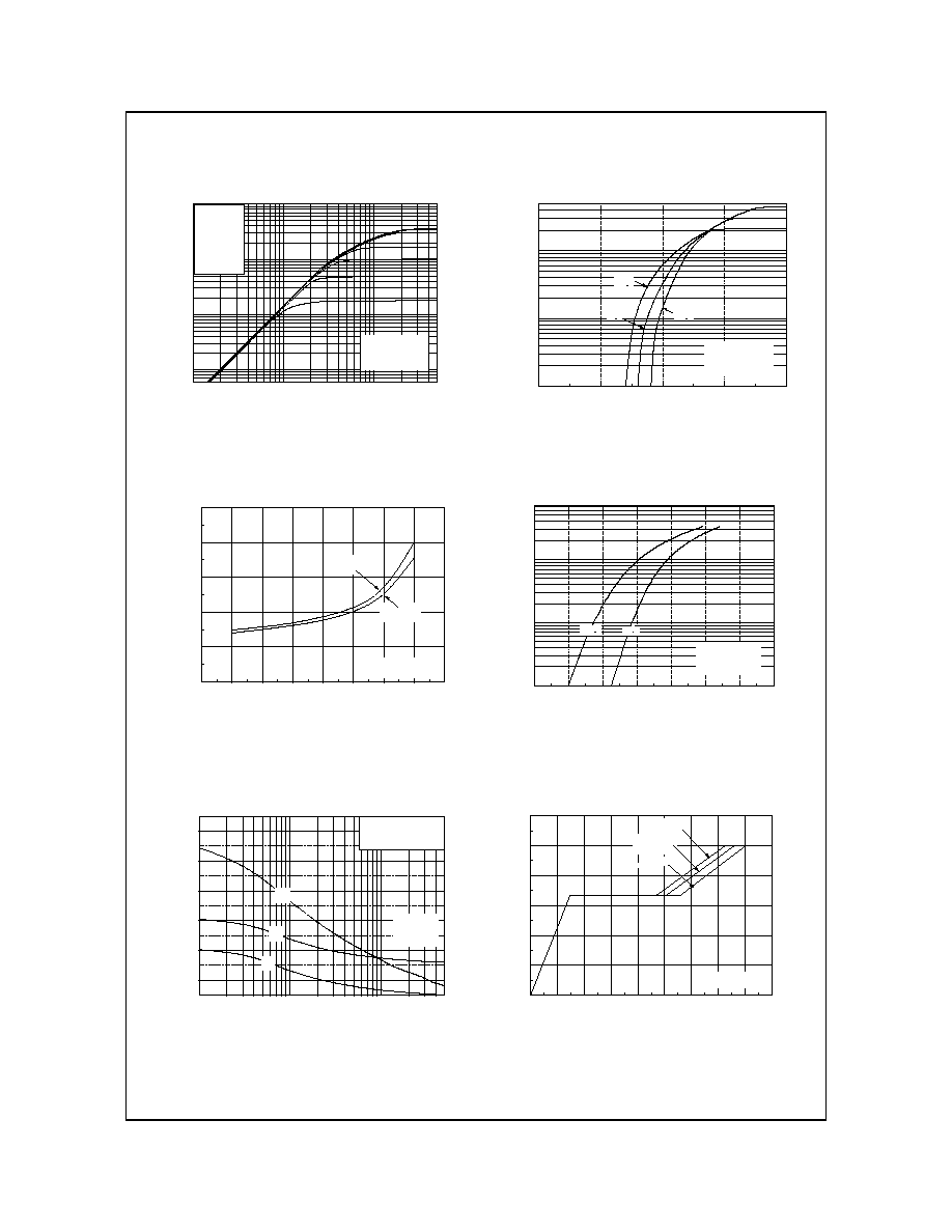
Typical Characteristics
Figure 5. Capacitance Characteristics
Figure 6. Gate Charge Characteristics
Figure 2. Transfer Characteristics
Figure 1. On-Region Characteristics
10
-1
10
0
10
1
10
-1
10
0
10
1
10
2
V
GS
Top : 15.0 V
10.0 V
8.0 V
7.0 V
6.5 V
6.0 V
Bottom : 5.5 V
* Notes :
1. 250
µ
s Pulse Test
2. T
C
= 25
o
C
I
D
,
D
r
ai
n C
u
r
r
en
t
[
A
]
V
DS
, Drain-Source Voltage [V]
2
4
6
8
10
10
-1
10
0
10
1
* Note
1. V
DS
= 40V
2. 250
µ
s Pulse Test
-55
o
C
150
o
C
25
o
C
I
D
,
D
r
a
i
n
C
u
r
r
e
n
t
[A
]
V
GS
, Gate-Source Voltage [V]
0
5
10
15
20
25
30
35
40
0.0
0.2
0.4
0.6
0.8
1.0
V
GS
= 20V
V
GS
= 10V
* Note : T
J
= 25
o
C
R
DS
(
O
N)
[
],
D
r
ai
n
-
S
o
ur
ce O
n
-
R
e
s
i
s
t
a
nce
I
D
, Drain Current [A]
10
-1
10
0
10
1
0
1000
2000
3000
4000
5000
6000
C
iss
= C
gs
+ C
gd
(C
ds
= shorted)
C
oss
= C
ds
+ C
gd
C
rss
= C
gd
* Notes :
1. V
GS
= 0 V
2. f = 1 MHz
C
rss
C
oss
C
iss
C
apaci
t
ance [
p
F]
V
DS
, Drain-Source Voltage [V]
0
5
10
15
20
25
30
35
40
45
0
2
4
6
8
10
12
V
DS
= 250V
V
DS
= 100V
V
DS
= 400V
* Note : I
D
= 11A
V
GS
,
G
a
t
e
-
S
our
ce V
o
l
t
age
[
V
]
Q
G
, Total Gate Charge [nC]
0.2
0.4
0.6
0.8
1.0
1.2
1.4
1.6
10
-1
10
0
10
1
25
o
C
150
o
C
* Notes :
1. V
GS
= 0V
2. 250
µ
s Pulse Test
I
DR
,
R
e
v
e
r
s
e D
r
ai
n C
u
r
r
en
t
[
A
]
V
SD
, Source-Drain Voltage [V]
Figure 3. On-Resistance Variation vs.
Drain Current and Gate Voltage
Figure 4. Body Diode Forward Voltage
Variation vs. Source Current
and Temperature
©2004 Fairchild Semiconductor Corporation
Rev. B, March 2004
FCP11N60
/FCPF11N60
Typical Characteristics
(Continued)
-100
-50
0
50
100
150
200
0.8
0.9
1.0
1.1
1.2
* Notes :
1. V
GS
= 0 V
2. I
D
= 250
µ
A
BV
DS
S
,
(N
o
r
m
a
liz
e
d
)
D
r
ai
n-
S
o
ur
c
e
Br
e
a
k
dow
n Vol
t
ag
e
T
J
, Junction Temperature [
o
C]
-100
-50
0
50
100
150
200
0.0
0.5
1.0
1.5
2.0
2.5
3.0
* Notes :
1. V
GS
= 10 V
2. I
D
= 5.5 A
R
DS
(
O
N)
,
(
N
or
m
a
l
i
zed)
D
r
ai
n-
Sour
ce O
n
-
R
esi
s
t
anc
e
T
J
, Junction Temperature [
o
C]
25
50
75
100
125
150
0.0
2.5
5.0
7.5
10.0
12.5
I
D
,
D
r
ai
n C
u
r
r
ent
[
A
]
T
C
, Case Temperature [
o
C]
Figure 7. Breakdown Voltage Variation
vs. Temperature
Figure 8. On-Resistance Variation
vs. Temperature
Figure 10. Maximum Drain Current
vs. Case Temperature
10
0
10
1
10
2
10
3
10
-2
10
-1
10
0
10
1
10
2
100 us
DC
100 ms
10 ms
1 ms
Operation in This Area
is Limited by R
DS(on)
* Notes :
1. T
C
= 25
o
C
2. T
J
= 150
o
C
3. Single Pulse
I
D
,
D
r
ai
n C
u
r
r
ent
[
A
]
V
DS
, Drain-Source Voltage [V]
10
0
10
1
10
2
10
3
10
-2
10
-1
10
0
10
1
10
2
Operation in This Area
is Limited by R
DS(on)
DC
10 ms
1 ms
100 us
* Notes :
1. T
C
= 25
o
C
2. T
J
= 150
o
C
3. Single Pulse
I
D
,
D
r
ai
n C
u
r
r
ent
[
A
]
V
DS
, Drain-Source Voltage [V]
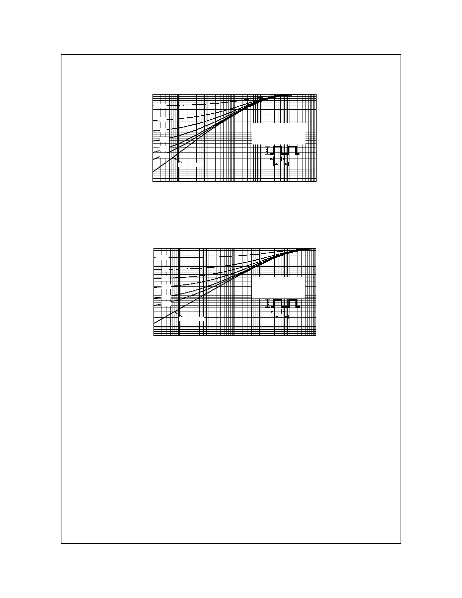
Figure 9-2. Maximum Safe Operating Area
for FCPF11N60
Figure 9-1. Maximum Safe Operating Area
for FCP11N60
Rev. B, March 2004
FCP11N60
/FCPF11N60
©2004 Fairchild Semiconductor Corporation
Typical Characteristics
(Continued)
1 0
-5
1 0
-4
1 0
-3
1 0
-2
1 0
-1
1 0
0
1 0
1
1 0
-2
1 0
-1
1 0
0
* N o te s :
1 . Z
J C
(t) = 1 .0
o
C /W M a x .
2 . D u ty F a c to r, D = t
1
/t
2
3 . T
J M
- T
C
= P
D M
* Z
J C
(t)
s in g le p u ls e
D = 0 .5
0 .0 2
0 .2
0 .0 5
0 .1
0 .0 1
Z
JC
(t
),
T
h
e
r
m
a
l
R
e
s
p
o
n
s
e
t
1
, S q u a re W a ve P u ls e D u ra tio n [s e c ]
t
1
P
DM
t
2
10
-5
10
-4
10
-3
10
-2
10
-1
10
0
10
1
10
-2
10
-1
10
0
* N o te s :
1 . Z
J C
(t) = 3 .5
o
C /W M a x .
2 . D u ty F a c to r, D = t
1
/t
2
3 . T
J M
- T
C
= P
D M
* Z
J C
(t)
sin g le p u ls e
D = 0 .5
0 .0 2
0 .2
0 .0 5
0 .1
0 .0 1
Z
JC
(
t
)
,
T
h
er
m
a
l
R
e
sponse
t
1
, S q u a re W a ve P u ls e D u ra tio n [se c]
Figure 11-1. Transient Thermal Response Curve for FCP11N60
Figure 11-2. Transient Thermal Response Curve for FCPF11N60
t
1
P
DM
t
2