 | ÐлекÑÑоннÑй компоненÑ: FDB5645 | СкаÑаÑÑ:  PDF PDF  ZIP ZIP |
Äîêóìåíòàöèÿ è îïèñàíèÿ www.docs.chipfind.ru
March 2000
©
2000 Fairchild Semiconductor Corporation
FDP5645/FDB5645 Rev B (W)
FDP5645/FDB5645
60V N-Channel PowerTrench
®
MOSFET
General Description
This N-Channel MOSFET has been designed
specifically to improve the overall efficiency of DC/DC
converters using either synchronous or conventional
switching PWM controllers.
These MOSFETs feature faster switching and lower
gate charge than other MOSFETs with comparable
R
DS(ON)
specifications.
The result is a MOSFET that is easy and safer to drive
(even at very high frequencies), and DC/DC power
supply designs with higher overall efficiency.
Features
·
80 A, 60 V.
R
DS(ON)
= 0.0095
@ V
GS
= 10 V
R
DS(ON)
= 0.011
@ V
GS
= 6 V.
·
Critical DC electrical parameters specified at
elevated temperature.
·
Rugged internal source-drain diode can eliminate the
need for an external Zener diode transient
suppressor.
·
High performance trench technology for extremely
low R
DS(ON)
.
·
175
°
C maximum junction temperature rating.
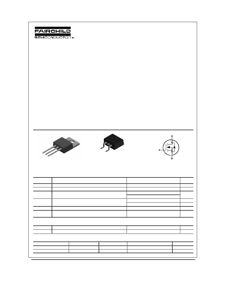
S
G
D
TO-220
FDP Series
D
G
S
TO-263AB
FDB Series
S
D
G
Absolute Maximum Ratings
T
A
=25
o
C unless otherwise noted
Symbol
Parameter
FDP5645 FDB5645
Units
V
DSS
Drain-Source Voltage
60
V
V
GSS
Gate-Source Voltage
±
20
V
I
D
Maximum Drain Current
Continuous (note 3)
80
A
Pulsed
300
Total Power Dissipation @ T
C
= 25
°
C
125
W
P
D
Derate above 25
°
C
0.83
W/
°
C
T
J
, T
STG
Operating and Storage Junction Temperature Range
-65 to +175
°
C
T
L
Maximum lead termperature for soldering purposes,
1/8" from case for 5 seconds
+275
°
C
Thermal Characteristics
R
JC
Thermal Resistance, Junction-to-Case
1.2
°
C/W
R
JA
Thermal Resistance, Junction-to-Ambient
62.5
°
C/W
Package Marking and Ordering Information
Device Marking
Device
Reel Size
Tape width
Quantity
FDB5645
FDB5645
13"
24mm
800 units
FDP5645
FDP5645
note 2
FDP5645/FDB5645
FDP5645/FDB5645 Rev. B (W)
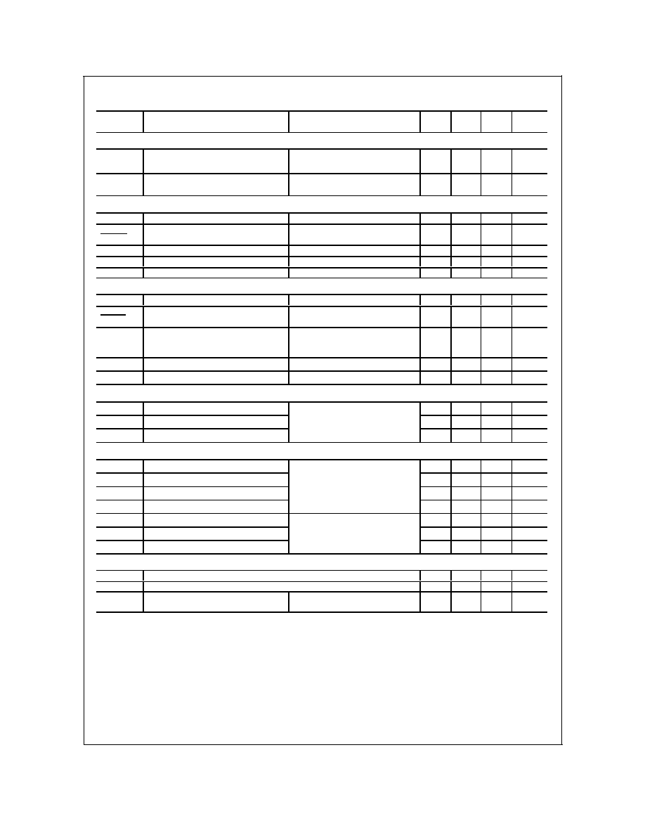
Electrical Characteristics
T
A
= 25°C unless otherwise noted
Symbol
Parameter
Test Conditions
Min
Typ Max Units
Drain-Source Avalanche Ratings
(Note 1)
W
DSS
Single Pulse Drain-Source
Avalanche Energy
V
DD
= 40 V,
I
D
= 80 A
800
mJ
I
AR
Maximum Drain-Source Avalanche
Current
80
A
Off Characteristics
BV
DSS
DrainSource Breakdown Voltage
V
GS
= 0 V, I
D
= 250
µ
A
60
V
BV
DSS
T
J
Breakdown Voltage Temperature
Coefficient
I
D
= 250
µ
A, Referenced to 25
°
C
64
mV/
°
C
I
DSS
Zero Gate Voltage Drain Current
V
DS
= 48 V,
V
GS
= 0 V
1
µ
A
I
GSSF
GateBody Leakage, Forward
V
GS
= 20 V,
V
DS
= 0 V
100
nA
I
GSSR
GateBody Leakage, Reverse
V
GS
= 20 V,
V
DS
= 0 V
100
nA
On Characteristics
(Note 1)
V
GS(th)
Gate Threshold Voltage
V
DS
= V
GS
, I
D
= 250
µ
A
2
4
V
V
GS(th)
T
J
Gate Threshold Voltage
Temperature Coefficient
I
D
= 250
µ
A, Referenced to 25
°
C
-7.8
mV/
°
C
R
DS(on)
Static DrainSource
OnResistance
V
GS
= 10 V,
I
D
= 40 A
V
GS
=10V, I
D
= 40 A, T
J
=125
°
C
V
GS
= 6 V,
I
D
= 38 A
8
13
9
9.5
18
11
m
I
D(on)
OnState Drain Current
V
GS
= 10 V,
V
DS
= 10 V
60
A
g
FS
Forward Transconductance
V
DS
= 5 V,
I
D
= 40 A
88
S
Dynamic Characteristics
C
iss
Input Capacitance
4468
pF
C
oss
Output Capacitance
810
pF
C
rss
Reverse Transfer Capacitance
V
DS
= 30 V,
V
GS
= 0 V,
f = 1.0 MHz
198
pF
Switching Characteristics
(Note 2)
t
d(on)
TurnOn Delay Time
21
30
ns
t
r
TurnOn Rise Time
13
20
ns
t
d(off)
TurnOff Delay Time
77
90
ns
t
f
TurnOff Fall Time
V
DD
= 30 V,
I
D
= 1 A,
V
GS
= 10 V,
R
GEN
= 6
42
50
ns
Q
g
Total Gate Charge
76
107
nC
Q
gs
GateSource Charge
18
nC
Q
gd
GateDrain Charge
V
DS
= 30 V,
I
D
= 80 A,
V
GS
= 10 V
21
nC
DrainSource Diode Characteristics and Maximum Ratings
I
S
Maximum Continuous DrainSource Diode Forward Current
80
A
I
S
Maximum Pulsed DrainSource Diode Forward Current
300
A
V
SD
DrainSource Diode Forward
Voltage
V
GS
= 0 V, I
S
= 40 A
0.9
1.3
V
Notes:
1.
Pulse Test: Pulse Width < 300
µ
s, Duty Cycle < 2.0%
2.
TO-220 package is supplied in tube / rail @ 45 pieces per rail.
3.
Calculated continuous current based on maximum allowable junction temperature. Actual maximum continuous current limited by package constraints to 75A
FDP5645/FDB5645
FDP5645/FDB5645 Rev. B (W)
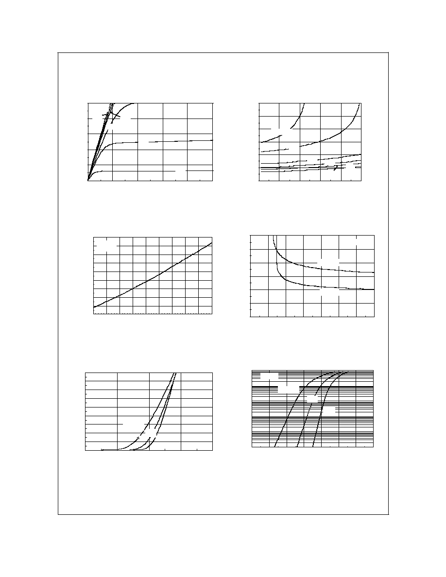
Typical Characteristics
0
20
40
60
80
100
0
1
2
3
4
5
V
DS
, DRAIN-SOURCE VOLTAGE (V)
I
D
, DRAIN-SOURCE CURRENT (A)
V
GS
= 10V
4.0V
5.0V
4.5V
6.0V
7.0V
0.8
1
1.2
1.4
1.6
1.8
2
0
20
40
60
80
100
I
D
, DRAIN CURRENT (A)
R
DS(ON)
, NORMALIZED
DRAIN-SOURCE ON-RESISTANCE
V
GS
= 4.5V
10V
5.0V
6.0V
7.0V
8.0V
Figure 1. On-Region Characteristics.
Figure 2. On-Resistance Variation with
Drain Current and Gate Voltage.
0.4
0.6
0.8
1
1.2
1.4
1.6
1.8
2
2.2
-50
-25
0
25
50
75
100
125
150
175
T
J
, JUNCTION TEMPERATURE (
o
C)
R
DS(ON)
, NORMALIZED
DRAIN-SOURCE ON-RESISTANCE
I
D
= 42A
V
GS
= 10V
0
0.004
0.008
0.012
0.016
0.02
0.024
3
4
5
6
7
8
9
10
V
GS
, GATE TO SOURCE VOLTAGE (V)
R
DS(ON)
, ON-RESISTANCE (OHM)
I
D
= 42A
T
A
= 125
o
C
T
A
= 25
o
C
Figure 3. On-Resistance Variation
withTemperature.
Figure 4. On-Resistance Variation with
Gate-to-Source Voltage.
0
10
20
30
40
50
60
70
80
90
2
3
4
5
6
V
GS
, GATE TO SOURCE VOLTAGE (V)
I
D
, DRAIN CURRENT (A)
T
A
= 125
o
C
25
o
C
-55
o
C
V
DS
= 5V
0.001
0.01
0.1
1
10
100
0
0.2
0.4
0.6
0.8
1
1.2
1.4
V
SD
, BODY DIODE FORWARD VOLTAGE (V)
I
S
, REVERSE DRAIN CURRENT (A)
T
A
= 125
o
C
25
o
C
-55
o
C
V
GS
= 0V
Figure 5. Transfer Characteristics.
Figure 6. Body Diode Forward Voltage Variation
with Source Current and Temperature.
FDP5645/FDB5645
FDP5645/FDB5645 Rev. B (W)
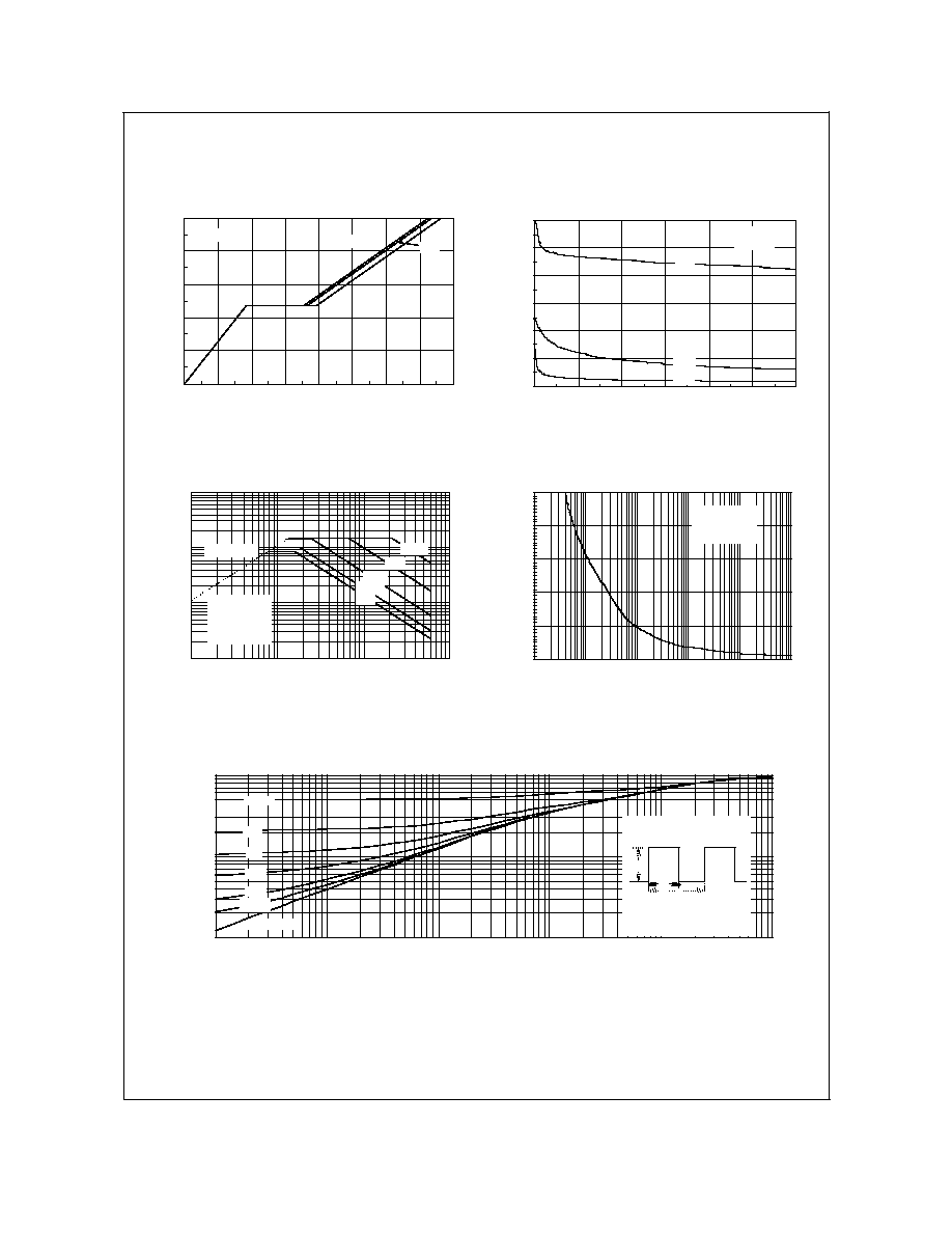
Typical Characteristics
0
2
4
6
8
10
0
10
20
30
40
50
60
70
80
Q
g
, GATE CHARGE (nC)
V
GS
, GATE-SOURCE VOLTAGE (V)
I
D
= 85A
V
DS
=
10V
20V
30V
0
1000
2000
3000
4000
5000
6000
0
10
20
30
40
50
60
V
DS
, DRAIN TO SOURCE VOLTAGE (V)
CAPACITANCE (pF)
C
ISS
C
RSS
C
OSS
f = 1MHz
V
GS
= 0 V
Figure 7. Gate Charge Characteristics.
Figure 8. Capacitance Characteristics.
1
10
100
1000
0.1
1
10
100
V
DS
, DRAIN-SOURCE VOLTAGE (V)
I
D
, DRAIN CURRENT (A)
R
DS(ON)
LIMIT
V
GS
= 10V
SINGLE PULSE
R
JC
= 1.2
o
C/W
T
C
= 25
o
C
DC
100ms
10ms
1ms
100
µ
s
0
1000
2000
3000
4000
5000
0.01
0.1
1
10
100
1000
SINGLE PULSE TIME (ms)
POWER (W)
SINGLE PULSE
R
JC
= 1.2
o
C/W
T
C
= 25
o
C
Figure 9. Maximum Safe Operating Area.
Figure 10. Single Pulse Maximum
Power Dissipation.
0.01
0.05
0.1
0.5
1
5
10
50
100
500
1000
0.01
0.02
0.03
0.05
0.1
0.2
0.3
0.5
1
t ,TIME (ms)
TRANSIENT THERMAL RESISTANCE
Single Pulse
D = 0.5
0.1
0.05
0.02
0.01
0.2
Duty Cycle, D = t / t
1
2
R (t) = r(t) * R
R = 1.2 °C/W
JC
JC
JC
T - T = P * R (t)
JC
C
J
P(pk)
t
1
t
2
r(t), NORMALIZED EFFECTIVE
1
Figure 11. Transient Thermal Response Curve.
Thermal characterization performed using the conditions described in Note 1c.
Transient thermal response will change depending on the circuit board design.
FDP5645/FDB5645
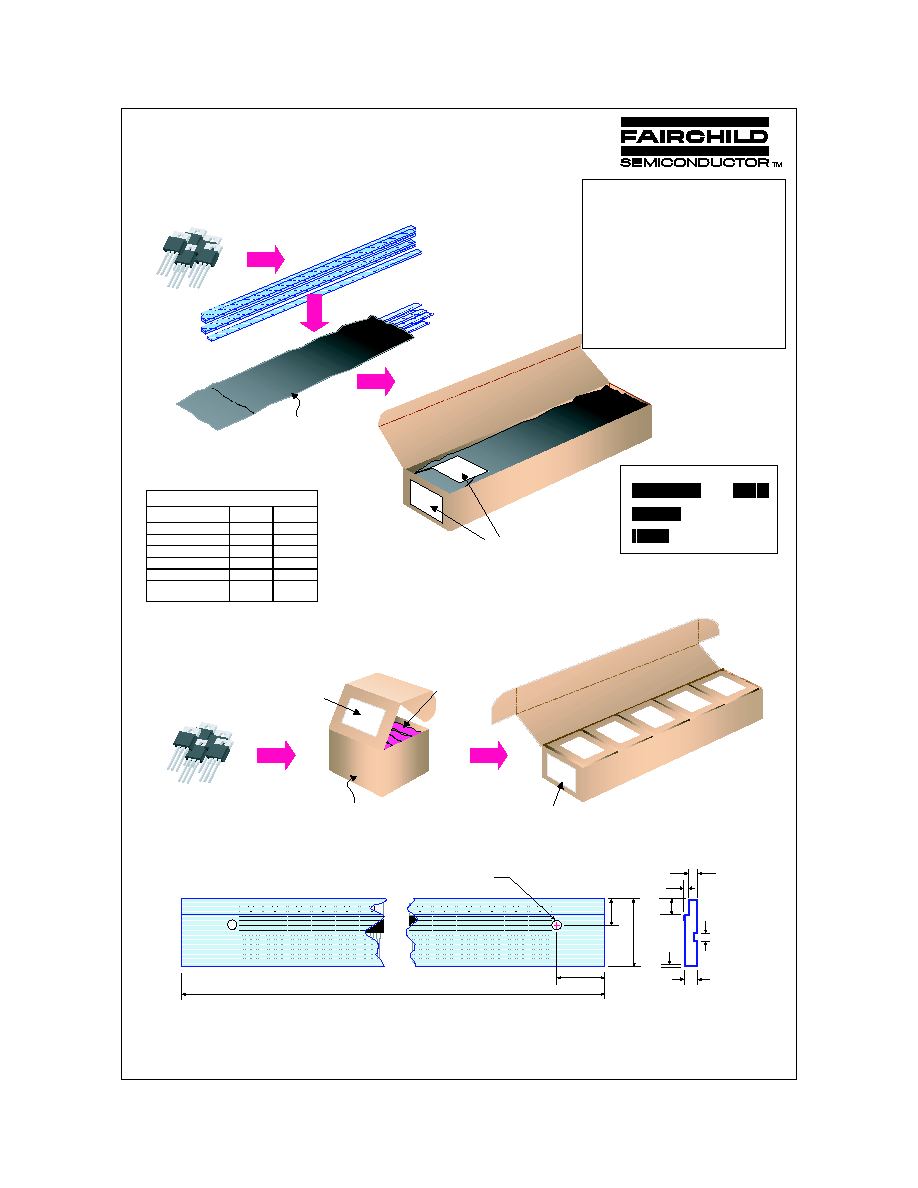
TO-220 Tape and Reel Data and Package Dimensions
August 1999, Rev. B
0.165
TO-220 Tube Packing
Configuration: Figur e 1.0
Note/Comments
Packaging Option
TO-220 Packaging Information
Standard
(no
f l ow code )
Packaging type
Rail/Tube
Qty per Tube/Box
45
Box Dimension (mm)
530x130x83
Max qty per Box
1,080
Weight per unit (gm)
1.4378
S62Z
BULK
300
114x102x51
1,500
1.4378
FSCINT Label
FSCINT Label
114mm x 102mm x 51mm
EO70 Immed iate Box
530mm x 130mm x 83mm
Intermediate bo x
300 units per
EO70 box
5 EO70 boxe s per per
Interm ediate Bo x
1500 uni ts maxi mum
qu ant it y per intermediate box
An ti-stati c
Bubbl e Sheet s
45 un it s per Tube
Conduct ive Plas ti c B ag
1080 uni ts maxi mum
qu ant it y per bo x
530mm x 130mm x 83mm
Intermediate bo x
FSCINT Label
12 Tube s per Bag
Note: All dim ensions are in inches
F9852
NDP4060L
F9852
NDP4060L
F9852
NDP4060L
F9852
NDP4060L
F9852
NDP4060L
F9852
NDP4060L
F9852
NDP4060L
F9852
NDP4060L
F9852
NDP4060L
F9852
NDP4060L
F9852
NDP4060L
F9852
NDP4060L
1.300
±
.015
0.080
0.032
±
.003
0.275
0.275
0.160
0.800
0.450
±
.030
20.000
+0.031
-0.065
0.123
+0.001
-0.003
LOT:
CBVK741B019
NSID:
FDP7060
D/C1:
D9842
SPEC REV:
B2
SPEC:
QTY:
1080
QA REV:
FAIRCHILD SEMICONDUCTOR CORPORATION
HTB:B
(FSCINT)
FSCINT Labe l samp le
TO-220 Tube
Configuration: Figure 4.0
TO-220 Packaging
Information: Figure 2.0
TO-220 bulk Packing
Configuration: Figure 3.0
2 bag s per Box
Packaging Description:
TO-220 parts are ship ped normally in tube. The tube is
made of PVC plastic treated with anti -stati c agent.These
tubes in standard option are placed inside a dissipative
plastic bag, barcode labeled, and placed inside a box
made of recyclable corrugated pa per. One box contains
two ba gs maximum (see fig. 1.0). And one or several o f
these boxes are placed inside a labeled shipp ing bo x
whic h c omes in different sizes dependi ng on the nu mber
of parts ship ped. The other option comes in bulk as
described in the Packagin g Information table. The unit s in
this option are placed inside a small box laid w ith anti-
static bubble sheet. These smaller boxes are individually
labeled and placed ins ide a larger box (see fig. 3.0).
These larger or intermediate boxes then will b e placed
finally inside a labeled shipping box whic h still comes in
different sizes depending on the number of units shipped.