 | ÐлекÑÑоннÑй компоненÑ: FDC6305N | СкаÑаÑÑ:  PDF PDF  ZIP ZIP |
Äîêóìåíòàöèÿ è îïèñàíèÿ www.docs.chipfind.ru
FDC6305N
FDC6305N, Rev. C
FDC6305N
Dual N-Channel 2.5V Specified PowerTrench
TM
MOSFET
General Description
These N-Channel low threshold 2.5V specified
MOSFETs are produced using Fairchild Semiconductor's
advanced PowerTrench process that has been
especially tailored to minimize on-state resistance and
yet maintain low gate charge for superior switching
performance.
Applications
·
Load switch
·
DC/DC converter
·
Motor driving
Features
·
2.7 A, 20 V. R
DS(ON)
= 0.08
@ V
GS
= 4.5 V
R
DS(ON)
= 0.12
@ V
GS
= 2.5 V
·
Low gate charge (3.5nC typical).
·
Fast switching speed.
·
High performance trench technology for extremely
low R
DS(ON)
.
·
SuperSOT
TM
-6 package: small footprint (72% smaller
than standard SO-8); low profile (1mm thick).
©
1999 Fairchild Semiconductor Corporation
Absolute Maximum Ratings
T
A
= 25°C unless otherwise noted
Symbol
Parameter
Ratings
Units
V
DSS
Drain-Source Voltage
20
V
V
GSS
Gate-Source Voltage
±
8
V
I
D
Drain Current
- Continuous
(Note 1a)
2.7
A
- Pulsed
8
P
D
Power Dissipation for Single Operation
(Note 1a)
0.96
W
(Note 1b)
0.9
(Note 1c)
0.7
T
J
, T
stg
Operating and Storage Junction Temperature Range
-55 to +150
°
C
Thermal Characteristics
R
JA
Thermal Resistance, Junction-to-Ambient
(Note 1a)
130
°
C/W
R
JC
Thermal Resistance, Junction-to-Case
(Note 1)
60
°
C/W
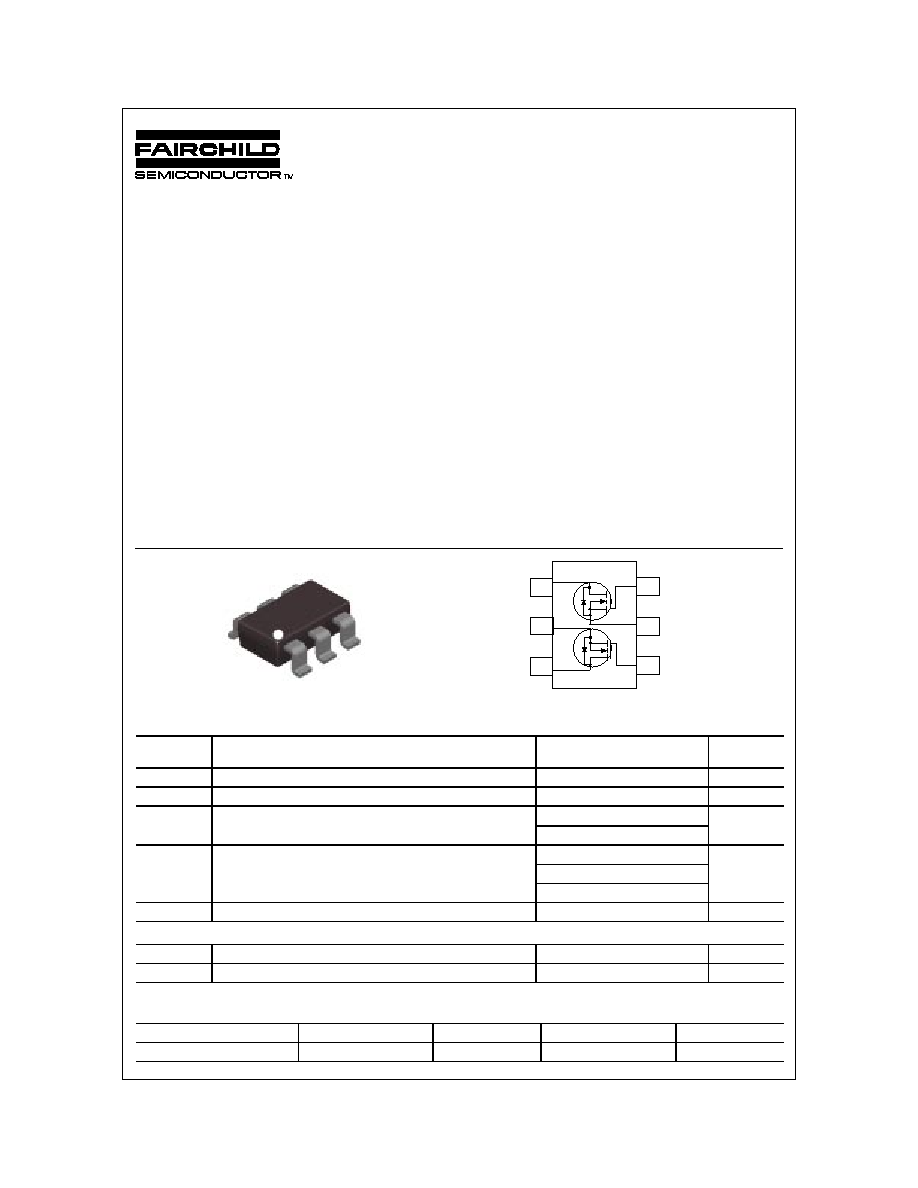
Package Outlines and Ordering Information
Device Marking
Device
Reel Size
Tape Width
Quantity
.305
FDC6305N
7''
8mm
3000 units
March 1999
1
5
3
2
6
4
D1
S2
G1
D2
S1
G2
SuperSOT -6
TM
FDC6305N
FDC6305N, Rev. C
Electrical Characteristics
T
A
= 25°C unless otherwise noted
Symbol
Parameter
Test Conditions
Min
Typ
Max Units
Off Characteristics
BV
DSS
Drain-Source Breakdown Voltage
V
GS
= 0 V, I
D
= 250
µ
A
20
V
BV
DSS
T
J
Breakdown Voltage Temperature
Coefficient
I
D
= 250
µ
A, Referenced to 25
°
C
14
mV/
°
C
I
DSS
Zero Gate Voltage Drain Current
V
DS
= 16 V, V
GS
= 0 V
1
µ
A
I
GSSF
Gate-Body Leakage Current, Forward
V
GS
= 8 V, V
DS
= 0 V
100
nA
I
GSSR
Gate-Body Leakage Current, Reverse
V
GS
= -8 V, V
DS
= 0 V
-100
nA
On Characteristics
(Note 2)
V
GS(th)
Gate Threshold Voltage
V
DS
= V
GS
, I
D
= 250
µ
A
0.4
0.9
1.5
V
V
GS(th)
T
J
Gate Threshold Voltage
Temperature Coefficient
I
D
= 250
µ
A, Referenced to 25
°
C
-2.7
mV/
°
C
R
DS(on)
Static Drain-Source
On-Resistance
V
GS
= 4.5, I
D
= 2.7 A
V
GS
= 4.5 I
D
= 2.7 A, T
J
= 125
°
C
V
GS
= 2.5 V, I
D
= 2.2 A
0.060
0.095
0.085
0.080
0.128
0.120
I
D(on)
On-State Drain Current
V
GS
= 4.5 V, V
DS
= 5 V
6
A
g
FS
Forward Transconductance
V
DS
= 5 V, I
D
= 2.7 A
8
S
Dynamic Characteristics
C
iss
Input Capacitance
310
pF
C
oss
Output Capacitance
80
pF
C
rss
Reverse Transfer Capacitance
V
DS
= 10 V, V
GS
= 0 V,
f = 1.0 MHz
40
pF
Switching Characteristics
(Note 2)
t
d(on)
Turn-On Delay Time
5
15
ns
t
r
Turn-On Rise Time
8.5
17
ns
t
d(off)
Turn-Off Delay Time
11
20
ns
t
f
Turn-Off Fall Time
V
DD
= 10 V, I
D
= 1 A,
V
GS
= 4.5 V, R
GEN
= 6
3
10
ns
Q
g
Total Gate Charge
3.5
5
nC
Q
gs
Gate-Source Charge
0.55
nC
Q
gd
Gate-Drain Charge
V
DS
= 10 V, I
D
= 2.7 A,
V
GS
= 4.5 V
0.95
nC
Drain-Source Diode Characteristics and Maximum Ratings
I
S
Maximum Continuous Drain-Source Diode Forward Current
0.8
A
V
SD
Drain-Source Diode Forward Voltage
V
GS
= 0 V, I
S
= 0.8 A
(Note 2)
0.77
1.2
V
Notes:
1. R
JA
is the sum of the junction-to-case and case-to-ambient resistance where the case thermal reference is defined as the solder mounting surface
of the drain pins. R
JC
is guaranteed by design while R
CA
is determined by the user's board design. Both devices are assumed to be operating and
sharing the dissipated heat energy equally.
Scale 1 : 1 on letter size paper
2. Pulse Test: Pulse Width
300
µ
s, Duty Cycle
2.0%
a) 130
°
C/W when
mounted on a 0.125 in
2
pad of 2 oz. copper.
b) 140
°
C/W when
mounted on a 0.005 in
2
pad of 2 oz. copper.
c) 180
°
C/W on a minimum
mounting pad.
FDC6305N
FDC6305N, Rev. C
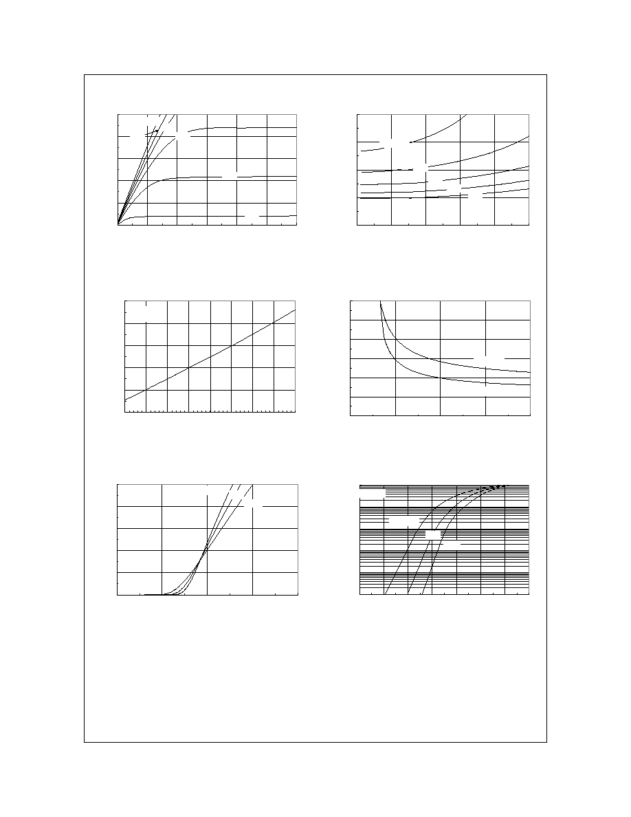
Typical Characteristics
Figure 1. On-Region Characteristics.
Figure 2. On-Resistance Variation
with Drain Current and Gate Voltage.
Figure 3. On-Resistance Variation
with Temperature.
Figure 4. On-Resistance Variation
with Gate-to-Source Voltage.
Figure 5. Transfer Characteristics.
Figure 6. Body Diode Forward Voltage
Variation with Source Current
and Temperature.
0.6
0.8
1
1.2
1.4
1.6
-50
-25
0
25
50
75
100
125
150
T
J
, JUNCTION TEMPERATURE (
o
C)
R
D
S(O
N
)
,
NO
RMALI
Z
E
D
DRA
I
N
-S
O
URC
E
O
N
-RE
S
I
S
TANCE
I
D
= 2.7A
V
GS
= 4.5V
0
0.04
0.08
0.12
0.16
0.2
0.24
1
2
3
4
5
V
GS
, GATE TO SOURCE VOLTAGE (V)
R
DS
(
O
N)
,
ON
-R
ESI
ST
A
N
C
E
(OH
M
)
I
D
= 1.4A
T
A
= 125
o
C
T
A
= 25
o
C
0
2
4
6
8
10
0
1
2
3
4
V
GS
, GATE TO SOURCE VOLTAGE (V)
I
D
,
DRA
I
N
C
URR
E
N
T (
A
)
T
A
= -55
o
C
25
o
C
125
o
C
V
DS
= 5V
0.0001
0.001
0.01
0.1
1
10
0
0.2
0.4
0.6
0.8
1
1.2
1.4
V
SD
, BODY DIODE FORWARD VOLTAGE (V)
I
S
,
RE
V
E
RS
E
DR
AI
N C
URR
E
N
T (
A
)
T
A
= 125
o
C
25
o
C
-55
o
C
V
GS
= 0V
0
2
4
6
8
10
0
0.5
1
1.5
2
2.5
3
V
DS
, DRAIN TO SOURCE VOLTAGE (V)
I
D
,
DRA
I
N
C
URR
E
N
T (
A
)
V
GS
= 4.5V
3.0V
2.5V
2.0V
1.5V
3.5V
0.8
1
1.2
1.4
1.6
0
2
4
6
8
10
I
D
, DRAIN CURRENT (A)
R
D
S(O
N
)
,
NO
RM
AL
I
Z
E
D
DRA
IN
-
S
O
URCE
O
N
-
R
E
S
I
S
T
A
N
C
E
V
GS
= 2.5V
4.0V
3.5V
4.5V
3.0V
FDC6305N
FDC6305N, Rev. C
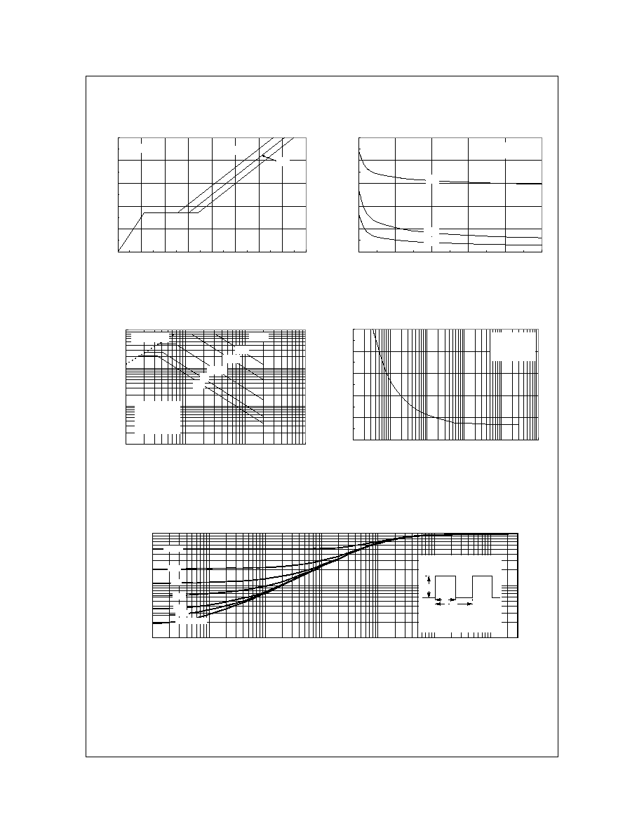
Typical Characteristics
(continued)
Figure 7. Gate-Charge Characteristics.
Figure 8. Capacitance Characteristics.
Figure 9. Maximum Safe Operating Area.
Figure 10. Single Pulse Maximum
Power Dissipation.
Figure 11. Transient Thermal Response Curve.
Thermal characterization performed using the conditions described in Note 1c.
Transient themal response will change depending on the circuit board design.
0.0001
0.001
0.01
0.1
1
10
100
300
0.01
0.02
0.05
0.1
0.2
0.5
1
t , TIME (sec)
T
R
A
N
S
I
EN
T
T
H
ER
M
A
L
R
ESI
ST
A
N
C
E
1
Single Pulse
D = 0.5
0.1
0.05
0.02
0.01
0.2
r
(
t
)
,
NO
RM
A
L
I
Z
E
D
E
F
F
E
CT
I
V
E
Duty Cycle, D = t / t
1
2
R (t) = r(t) * R
R = 180°C/W
JA
JA
JA
T - T = P * R (t)
JA
A
J
P(pk)
t
1
t
2
0
1
2
3
4
5
0
0.5
1
1.5
2
2.5
3
3.5
4
Q
g
, GATE CHARGE (nC)
V
GS
,
G
A
TE
-
S
O
URCE
V
O
LTAG
E
(V
)
I
D
= 2.7A
V
DS
= 5V
10V
15V
0
100
200
300
400
500
0
4
8
12
16
20
V
DS
, DRAIN TO SOURCE VOLTAGE (V)
CAP
ACI
TA
NCE
(pF)
C
ISS
C
RSS
C
OSS
f = 1MHz
V
GS
= 0 V
0.01
0.1
1
10
0.1
1
10
100
V
DS
, DRAIN-SOURCE VOLTAGE (V)
I
D
,
DRA
I
N
CURRE
NT (A)
DC
1s
100ms
10ms
1ms
100
µ
s
R
DS(ON)
LIMIT
V
GS
= 4.5V
SINGLE PULSE
R
JA
= 180
o
C/W
TA = 25
o
C
0
1
2
3
4
5
0.01
0.1
1
10
100
1000
SINGLE PULSE TIME (SEC)
PO
W
E
R
(
W
)
SINGLE PULSE
R
JA
= 180
o
C/W
T
A
= 25
o
C
1998 Fairchild Semiconductor Corporation
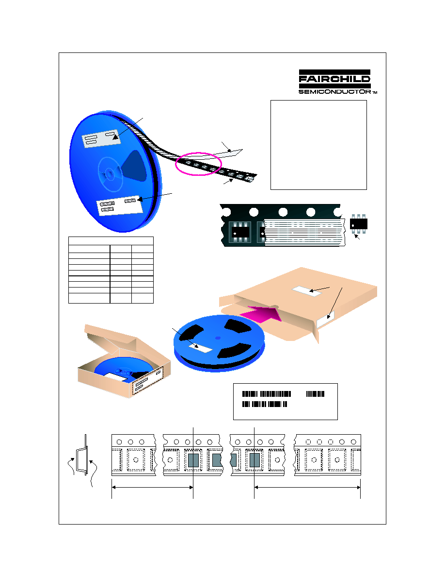
Embo ssed
Carrier Tape
SSOT-6 Packaging
Configuration: Figur e 1.0
Comp onent s
Lead er Tape
500mm mi nimum or
125 emp ty poc kets
Traile r Tape
300mm mi nimum or
75 empty poc kets
SSOT-6 Tape Leader and Trailer
Configuration: Figur e 2.0
Cover Tape
Carrier Tape
Note/Comments
Packaging Option
SSOT-6 Packaging Information
Standard
(no
f l ow c ode )
D87Z
Packaging type
Reel Size
TNR
7" Dia
TNR
13"
Qty per Reel/Tube/Bag
3,000
10,000
Box Dimension (mm)
184x187x47
343x343x64
Max qty per Box
9,000
30,000
Weight per unit (gm)
0.0158
0.0158
Weight per Reel (kg)
0.1440
0.4700
F63TNR
Label
Customize Lab el
Anti static Cover Tape
184mm x 187mm x 47mm
Pizza Box fo r Standar d Opti on
F63TNR
Label
F63TNR Labe l
F63TNR Labe l sa mpl e
343mm x 342mm x 64mm
Intermediate bo x fo r D87Z Option
F63TNR
Label
SSOT-6 Unit Orientation
631
631
631
631
631
Pin 1
LOT: CBVK741B019
FSID: FDC633N
D/C1: D9842 QTY1:
SPEC REV:
SPEC:
QTY: 3000
D/C2:
QTY2:
CPN:
N/F: F (F63TNR)3
Packaging Description:
SSOT-6 parts are shipped in tape. The carrier tape is
made from a dissipative (carbon filled) polycarbonate
resin. The cover tape is a multilayer film (Heat Activated
Adhesive in nature) primarily composed of polyester film,
adhesive layer, sealant, and anti-static sprayed agent.
These reeled parts in standard option are shipped with
3,000 units per 7" or 177cm diameter reel. The reels are
dark blue in color and is made of polystyrene plastic (anti-
static coated). Other option comes in 10,000 units per 13"
or 330cm diameter reel. This and some other options are
described in the Packaging Information table.
These full reels are individually barcode labeled and
placed inside a pizza box (illustrated in figure 1.0) made of
recyclable corrugated brown paper with a Fairchild logo
printing. One pizza box contains three reels maximum.
And these pizza boxes are placed inside a barcode
labeled shipping box which comes in different sizes
depending on the number of parts shipped.
SuperSOT
TM
-6 Tape and Reel Data and Package Dimensions
August 1999, Rev. C