 | ÐлекÑÑоннÑй компоненÑ: FDC6321C | СкаÑаÑÑ:  PDF PDF  ZIP ZIP |
Äîêóìåíòàöèÿ è îïèñàíèÿ www.docs.chipfind.ru
April 1999
FDC6321C
Dual N & P Channel , Digital FET
General Description Features
Absolute Maximum Ratings
T
A
= 25
o
C unless other wise noted
Symbol
Parameter
N-Channel
P-Channel
Units
V
DSS
, V
CC
Drain-Source Voltage, Power Supply Voltage
25
-25
V
V
GSS
, V
IN
Gate-Source Voltage,
8
-8
V
I
D
, I
O
Drain/Output Current
- Continuous
0.68
-0.46
A
- Pulsed
2
-1.5
P
D
Maximum Power Dissipation
(Note 1a)
(Note 1b)
0.9
W
0.7
T
J
,T
STG
Operating and Storage Tempature Ranger
-55 to 150
°C
ESD
Electrostatic Discharge Rating MIL-STD-883D
Human Body Model (100pf / 1500 Ohm)
6
kV
THERMAL CHARACTERISTICS
R
JA
Thermal Resistance, Junction-to-Ambient
(Note 1a)
140
°C/W
R
JC
Thermal Resistance, Junction-to-Case
(Note 1)
60
°C/W
FDC6321C.RevB
N-Ch 25 V, 0.68 A, R
DS(ON)
= 0.45
@ V
GS
= 4.5 V
P-Ch -25 V, -0.46 A, R
DS(ON)
= 1.1
@ V
GS
= -4.5 V.
Very low level gate drive requirements allowing direct
operation in 3 V circuits. V
GS(th)
< 1.0V.
Gate-Source Zener for ESD ruggedness.
>6kV Human Body Model
Replace multiple dual NPN & PNP digital transistors.
These dual N & P Channel logic level enhancement mode
field effect transistors are produced using Fairchild's
proprietary, high cell density, DMOS technology. This very
high density process is especially tailored to minimize
on-state resistance. This device has been designed
especially for low voltage applications as a replacement for
digital transistors in load switching applications. Since bias
resistors are not required this dual digital FET can replace
several digital transistors with different bias resistors.
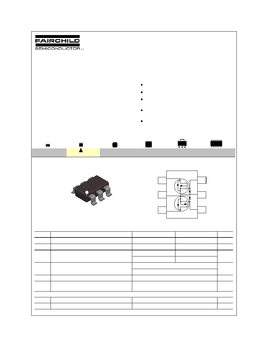
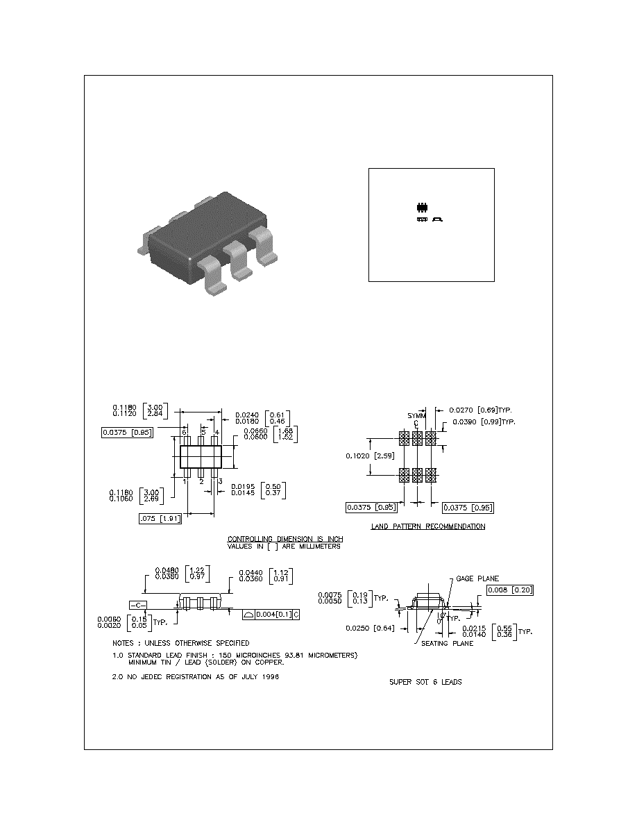
SOT-23
SuperSOT
TM
-8
SOIC-16
SO-8
SOT-223
SuperSOT
TM
-6
Mark:.321
1
5
3
2
6
4
D1
S2
G1
D2
S1
G2
SuperSOT -6
TM
© 1999 Fairchild Semiconductor Corporation
Electrical Characteristics
(T
A
= 25
O
C unless otherwise noted )
Symbol
Parameter
Conditions
Type
Min
Typ
Max
Units
OFF CHARACTERISTICS
BV
DSS
Drain-Source Breakdown Voltage
V
GS
= 0 V, I
D
= 250 µA
N-Ch
25
V
V
GS
= 0 V, I
D
= -250 µA
P-Ch
-25
BV
DSS
/
T
J
Breakdown Voltage Temp. Coefficient
I
D
= 250 µA, Referenced to 25
o
C
N-Ch
26
mV /
o
C
I
D
= -250 µA, Referenced to 25
o
C
P-Ch
-22
I
DSS
Zero Gate Voltage Drain Current
V
DS
= 20 V, V
GS
= 0 V,
N-Ch
1
µA
T
J
= 55°C
10
I
DSS
Zero Gate Voltage Drain Current
V
DS
=-20 V, V
GS
= 0 V,
P-Ch
-1
µA
T
J
= 55°C
-10
I
GSS
Gate - Body Leakage Current
V
GS
= 8 V, V
DS
= 0 V
N-Ch
100
nA
V
GS
= -8 V, V
DS
= 0 V
P-Ch
-100
nA
ON CHARACTERISTICS
(Note 2)
V
GS(th)
/
T
J
Gate Threshold Voltage Temp. Coefficient
I
D
= 250 µA, Referenced to 25
o
C
N-Ch
-2.6
mV /
o
C
I
D
= -250 µA, Referenced to 25
o
C
P-Ch
2.1
V
GS(th)
Gate Threshold Voltage
V
DS
= V
GS
, I
D
= 250 µA
N-Ch
0.65
0.8
1.5
V
V
DS
= V
GS
, I
D
= -250 µA
P-Ch
-0.65
-0.86
-1.5
R
DS(ON)
Static Drain-Source On-Resistance
V
GS
= 4.5 V, I
D
= 0.5 A
N-Ch
0.33
0.45
T
J
=125°C
0.51
0.72
V
GS
= 2.7 V, I
D
= 0.25A
0.44
0.6
V
GS
= -4.5 V, I
D
= -0.5 A
P-Ch
0.87
1.1
T
J
=125°C
1.21
1.8
V
GS
= -2.7 V, I
D
= -0.25 A
1.22
1.5
I
D(ON)
On-State Drain Current
V
GS
= 4.5 V, V
DS
= 5 V
N-Ch
1
A
V
GS
= -4.5 V, V
DS
= -5 V
P-Ch
-1
g
FS
Forward Transconductance
V
DS
= 5 V, I
D
= 0.5 A
N-Ch
1.45
S
V
DS
= -5 V, I
D
= -0.5 A
P-Ch
0.8
DYNAMIC CHARACTERISTICS
C
iss
Input Capacitance
N-Channel
N-Ch
50
pF
V
DS
= 10 V, V
GS
= 0 V,
P-Ch
63
C
oss
Output Capacitance
f = 1.0 MHz
N-Ch
28
pF
P-Channel
P-Ch
34
C
rss
Reverse Transfer Capacitance
V
DS
= -10 V, V
GS
= 0V,
N-Ch
9
pF
f = 1.0 MHz
P-Ch
10
FDC6321C.RevB
Electrical Characteristics
(T
A
= 25
O
C unless otherwise noted )
SWITCHING CHARACTERISTICS
(Note 2)
Symbol
Parameter
Conditions
Type
Min
Typ
Max
Units
t
D(on)
Turn - On Delay Time
N-Channel
N-Ch
3
6
nS
V
DD
= 6 V, I
D
= 0.5 A,
P-Ch
7
20
t
r
Turn - On Rise Time
V
Gs
= 4.5 V, R
GEN
= 50
N-Ch
8
16
nS
P-Ch
9
18
t
D(off)
Turn - Off Delay Time
P-Channel
N-Ch
17
30
nS
V
DD
= -6 V, I
D
= -0.5 A,
P-Ch
55
110
t
f
Turn - Off Fall Time
V
Gen
= -4.5 V, R
GEN
= 50
N-Ch
13
25
nS
P-Ch
35
70
Q
g
Total Gate Charge
N-Channel
N-Ch
1.64
2.3
nC
V
DS
= 5 V, I
D
= 0.5 A,
P-Ch
1.1
1.5
Q
gs
Gate-Source Charge
V
GS
= 4.5 V
N-Ch
0.38
nC
P- Channel
P-Ch
0.32
Q
gd
Gate-Drain Charge
V
DS
= -5 V,
N-Ch
0.45
nC
I
D
= -0.25 A, V
GS
= -4.5 V
P-Ch
0.25
DRAIN-SOURCE DIODE CHARACTERISTICS AND MAXIMUM RATINGS
I
S
Maximum Continuous Drain-Source Diode Forward Current
N-Ch
0.3
A
P-Ch
-0.5
V
SD
Drain-Source Diode Forward Voltage
V
GS
= 0 V, I
S
= 0.5 A
(Note)
N-Ch
0.83
1.2
V
T
J
=125°C
0.69
0.85
V
GS
= 0 V, I
S
= -0.5 A
(Note)
P-Ch
-0.89
-1.2
T
J
=125°C
-0.75
-0.85
Notes:
1. R
JA
is the sum of the junction-to-case and case-to-ambient thermal resistance where thecase thermal reference is defined as the solder mounting surface of the drain pins. R
JC
is guaranteed
by design while R
CA
is determined by the user's board design.
2. Pulse Test: Pulse Width < 300µs, Duty Cycle < 2.0%.
FDC6321C.RevB
b. 180
O
C/W on a 0.005 in
2
of pad
of 2oz copper.
a. 140
O
C/W on a 0.125 in
2
pad of
2oz copper.
FDC6321C.RevB
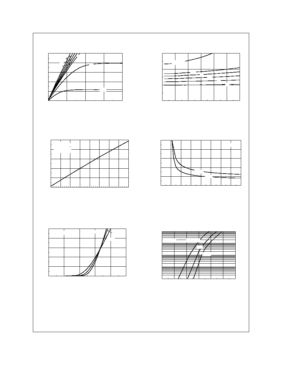
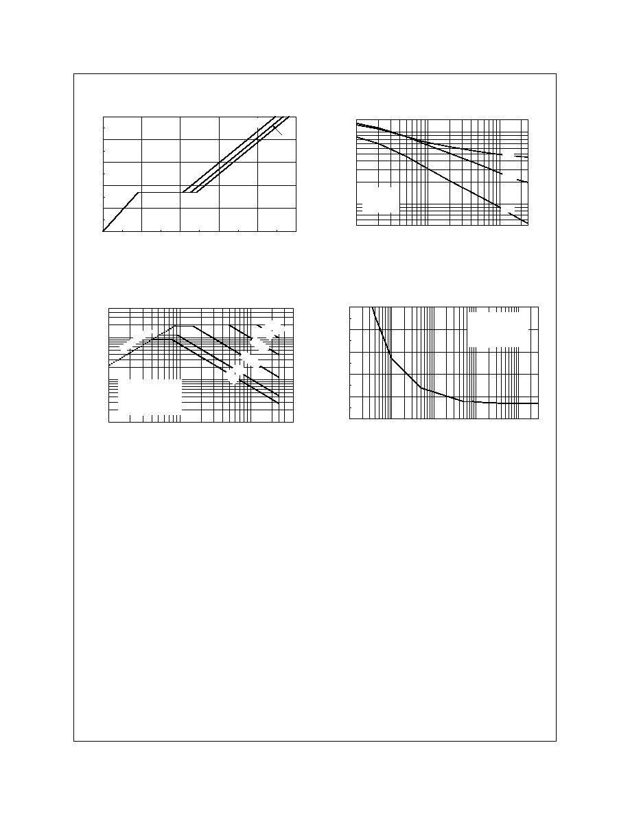
Typical Electrical Characteristics: N-Channel
0
0.5
1
1.5
2
0
0.3
0.6
0.9
1.2
1.5
V , DRAIN-SOURCE VOLTAGE (V)
I , DRAIN-SOURCE CURRENT (A)
3.5
2.7
2.5
2.0
1.5
DS
D
V = 4.5V
GS
3.0
R
DS(on
)
, NORMALIZED
0
0.2
0.4
0.6
0.8
1
1.2
0.5
1
1.5
2
I , DRAIN CURRENT (A)
DRAIN-SOURCE ON-RESISTANCE
V = 2.0V
GS
2.7
3.0
4.5
D
3.5
2.5
Figure 1. On-Region Characteristics.
Figure 2. On-Resistance Variation with
Drain Current and Gate Voltage.
-50
-25
0
25
50
75
100
125
150
0.6
0.8
1
1.2
1.4
1.6
T , JUNCTION TEMPERATURE (°C)
DRAIN-SOURCE ON-RESISTANCE
J
V = 4.5 V
GS
I =0.5 A
D
R , NORMALIZED
DS(ON)
Figure 3. On-Resistance Variation
with Temperature.
0
0.5
1
1.5
2
2.5
0
0.2
0.4
0.6
0.8
1
V , GATE TO SOURCE VOLTAGE (V)
I , DRAIN CURRENT (A)
25°C
125°C
V = 5.0V
DS
GS
D
T = -55°C
J
Figure 5. Transfer Characteristics.
0
0.2
0.4
0.6
0.8
1
1.2
0.0001
0.001
0.01
0.1
1
V , BODY DIODE FORWARD VOLTAGE (V)
I , REVERSE DRAIN CURRENT (A)
T = 125°C
J
25°C
-55°C
V = 0V
GS
SD
S
Figure 6. Body Diode Forward Voltage
Variation with Source Current and
Temperature.
Figure 4. On Resistance Variation with
Gate-To-Source Voltage.
1
1.5
2
2.5
3
3.5
4
4.5
5
0
0.4
0.8
1.2
1.6
2
V , GATE TO SOURCE VOLTAGE (V)
ID= 0.5A
GS
R , ON-RESISTANCE (OHM)
DS(on)
125°C
25°C
FDC6321C.RevB
Typical Electrical Characteristics: N-Channel
(continued)
0
0.4
0.8
1.2
1.6
2
0
1
2
3
4
5
Q , GATE CHARGE (nC)
V , GATE-SOURCE VOLTAGE (V)
g
GS
I = 0.5A
D
10V
15V
V = 5V
DS
Figure 10. Single Pulse Maximum Power
Dissipation.
0.1
0.5
1
2
5
10
25
5
10
20
50
100
150
V , DRAIN TO SOURCE VOLTAGE (V)
CAPACITANCE (pF)
DS
C
iss
f = 1 MHz
V = 0V
GS
C
oss
C
rss
Figure 8. Capacitance Characteristics.
Figure 7. Gate Charge Characteristics.
Figure 9. Maximum Safe Operating Area.
0.01
0.1
1
10
100
300
0
1
2
3
4
5
SINGLE PULSE TIME (SEC)
POWER (W)
SINGLE PULSE
R =See note 1b
T = 25°C
JA
A
0.1
0.2
0.5
1
2
5
10
20
40
0.01
0.03
0.1
0.3
1
5
V , DRAI N-SOURCE VOLTAGE (V)
I , DRAIN CURRENT (A)
V = 4.5V
SINGLE PULSE
R = See note 1b
T = 25°C
GS
JA
DS
D
DC
1s
10ms
100ms
RDS(ON) LIMIT
A
1ms
100µs
FDC6321C.RevB
Typical Electrical Characteristics: P-Channel
0
1
2
3
4
5
0
0.25
0.5
0.75
1
1.25
1.5
-V , DRAIN-SOURCE VOLTAGE (V)
-I , DRAIN-SOURCE CURRENT (A)
V = -4.5V
GS
DS
D
-2.7
-2.5
-2.0
-3.0
-1.5
-3.5
0
0.2
0.4
0.6
0.8
1
0.8
1
1.2
1.4
1.6
1.8
2
2.2
2.4
-I , DRAIN CURRENT (A)
DRAIN-SOURCE ON-RESISTANCE
V = -2.0 V
GS
D
R , NORMALIZED
DS(ON)
-3.5
-4.5
-2.7
-2.5
-3.0
-4.0
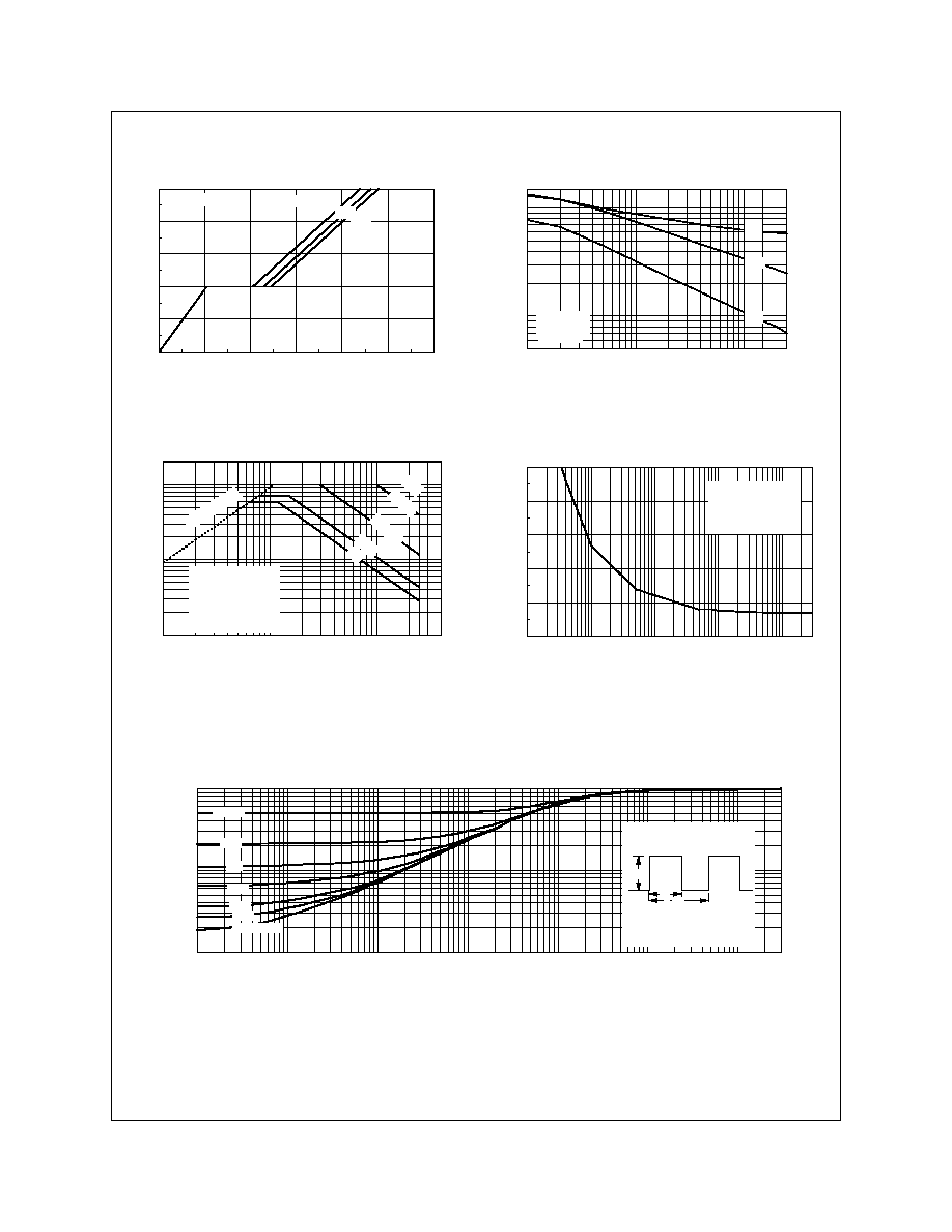
Figure 11. On-Region Characteristics.
Figure 12. On-Resistance Variation with
Drain Current and Gate Voltage.
-50
-25
0
25
50
75
100
125
150
0.6
0.8
1
1.2
1.4
1.6
T , JUNCTION TEMPERATURE (°C)
DRAIN-SOURCE ON-RESISTANCE (OHMS)
J
R , NORMALIZED
DS(ON)
V = -4.5V
GS
I = -0.5A
D
Figure 13. On-Resistance Variation
with Temperature.
-3
-2.5
-2
-1.5
-1
-0.5
-1
-0.75
-0.5
-0.25
0
V , GATE TO SOURCE VOLTAGE (V)
I , DRAIN CURRENT (A)
V = -5 V
DS
GS
D
T = -55°C
J
125°C
25°C
Figure 15. Transfer Characteristics.
0
0.2
0.4
0.6
0.8
1
1.2
0.0001
0.001
0.01
0.1
0.5
-V , BODY DIODE FORWARD VOLTAGE (V)
-I , REVERSE DRAIN CURRENT (A)
T = 125°C
J
25°C
-55°C
V = 0V
GS
SD
S
Figure 16. Body Diode Forward Voltage
Variation with Source Current and
Temperature.
Figure 14. On Resistance Variation with
Gate-To- Source Voltage.
-5
-4.5
-4
-3.5
-3
-2.5
-2
-1.5
-1
0
1
2
3
4
5
V , GATE TO SOURCE VOLTAGE (V)
ID=-0.5A
GS
R , ON-RESISTANCE (OHM)
DS(on)
125°C
25°C
FDC6321C.RevB
Typical Electrical Characteristics: P-Channel (continued)
Figure 19. Maximum Safe Operating Area.
0
0.3
0.6
0.9
1.2
1.5
1.8
0
1
2
3
4
5
Q , GATE CHARGE (nC)
-V , GATE-SOURCE VOLTAGE (V)
g
GS
I = -0.5A
D
-15V
V = -5V
DS
-10V
Figure 17. Gate Charge Characteristics.
Figure 20. Single Pulse Maximum Power
Dissipation.
0.1
0.3
0.5
1
5
10
15
25
5
10
20
50
100
150
-V , DRAIN TO SOURCE VOLTAGE (V)
CAPACITANCE (pF)
DS
C
iss
f = 1 MHz
V = 0 V
GS
C
oss
C
rss
Figure 18. Capacitance Characteristics.
Figure 21. Transient Thermal Response Curve.
Note: Thermal characterization performed using the conditions described in note 1b.Transient thermal
response will change depending on the circuit board design.
0.0001
0.001
0.01
0.1
1
10
100
300
0.01
0.02
0.05
0.1
0.2
0.5
1
t , TIME (sec)
TRANSIENT THERMAL RESISTANCE
1
Single Pulse
D = 0.5
0.1
0.05
0.02
0.01
0.2
r(t), NORMALIZED EFFECTIVE
Duty Cycle, D = t / t
1
2
R (t) = r(t) * R
R = See Note 1b
JA
JA
JA
T - T = P * R (t)
JA
A
J
P(pk)
t
1
t
2
0.01
0.1
1
10
100
300
0
1
2
3
4
5
SINGLE PULSE TIME (SEC)
POWER (W)
SINGLE PULSE
R =See note 1b
T = 25°C
JA
A
0.1
0.2
0.5
1
2
5
10
20
40
0.01
0.03
0.1
0.3
1
2
- V , DRAIN-SOURCE VOLTAGE (V)
-I , DRAIN CURRENT (A)
RDS(ON) LIMIT
D
A
DC
DS
1s
100ms
10ms
1ms
V = -4.5V
SINGLE PULSE
R = See Note 1b
T = 25°C
JA
GS
A
©
1998 Fairchild Semiconductor Corporation
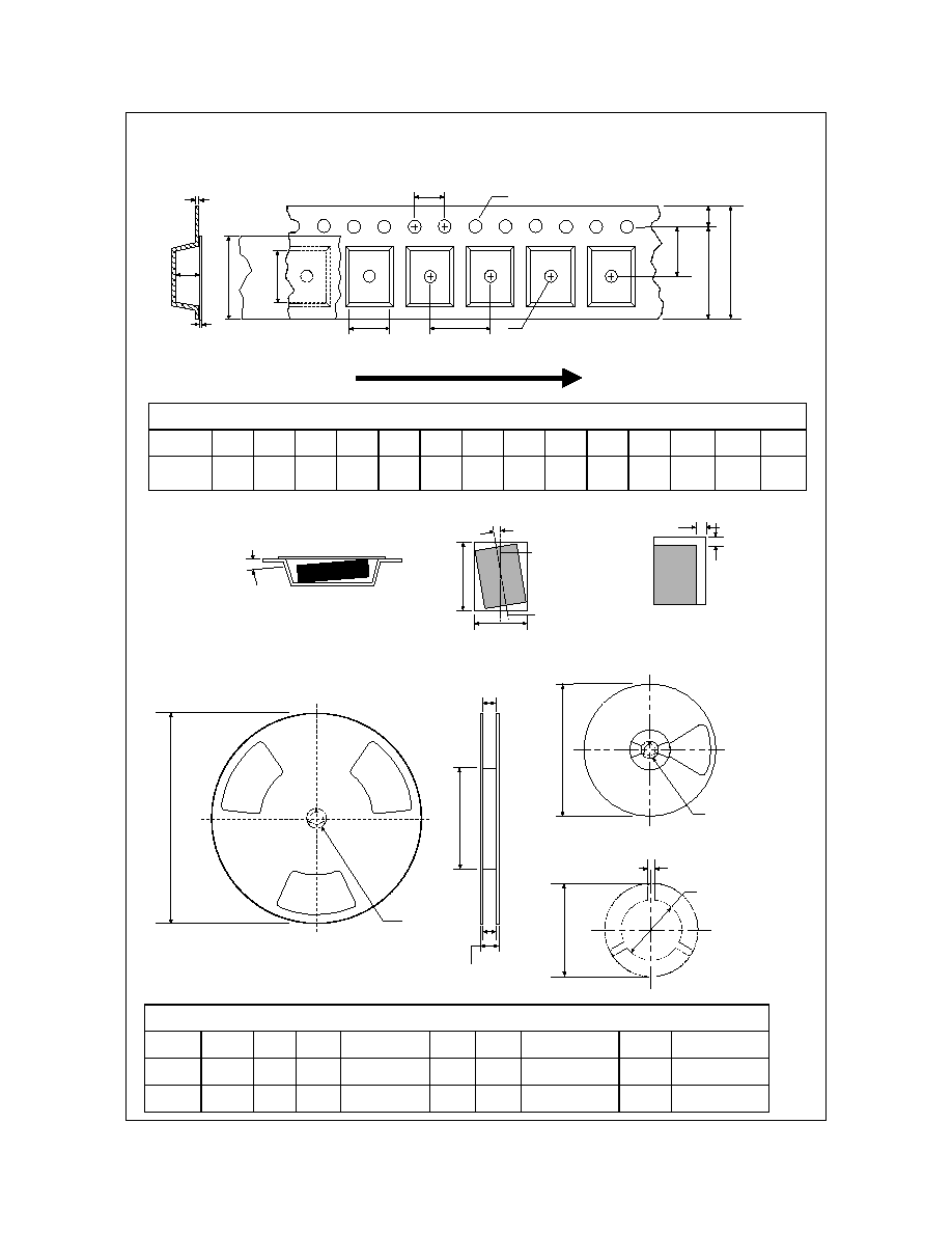
SSOT-6 Unit Orientation
Conductive Embossed
Carrier Tape
F63TNR
Label
Customize Label
Antistatic Cover Tape
SSOT-6 Packaging
Configuration: Figure 1.0
Components
Leader Tape
390mm minimum
Trailer Tape
160mm minimum
SSOT-6 Tape Leader
Trailer
Configuration: Figure 2.0
Cover Tape
Carrier
Pin 1
Tape
Note/Comments
Packaging Option
SSOT-6 Packaging Information
Standard
(no flow code)
D87Z
Packaging type
Reel Size
TNR
7" Dia
TNR
13"
Qty per Reel/Tube/Bag
3,000
10,000
Box Dimension (mm)
184x187x47
343x343x64
Max qty per Box
9,000
20,000
Weight per unit (gm)
0.0158
0.0158
Weight per Reel (kg)
0.1440
0.4700
184mm x 184mm x 47mm
Pizza Box for Standard Option
F63TNR
Label
F63TNR Label
F63TNR Label sample
343mm x 342mm x 64mm
Intermediate box for D87Z Option
631
631
631
631
LOT: CBVK741B019
FSID: FDC633N
D/C1: D9842
QTY1:
SPEC REV: QARV:
SPEC:
QTY: 3000
D/C2:
QTY2:
CPN:
(F63TNR)2
F63TNR
Label
SuperSOT
TM
-6 Tape and Reel Data and Package Dimensions
December 1998, Rev. B
P1
A0
D1
P0
F
W
E1
D0
E2
B0
Tc
Wc
K0
T
Dimensions are in inches and millimeters
Tape Size
Reel
Option
Dim A
Dim B
Dim C
Dim D
Dim N
Dim W1
Dim W2
Dim W3 (LSL-USL)
8mm
7" Dia
7.00
177.8
0.059
1.5
512 +0.020/-0.008
13 +0.5/-0.2
0.795
20.2
2.165
55
0.331 +0.059/-0.000
8.4 +1.5/0
0.567
14.4
0.311 0.429
7.9 10.9
8mm
13" Dia
13.00
330
0.059
1.5
512 +0.020/-0.008
13 +0.5/-0.2
0.795
20.2
4.00
100
0.331 +0.059/-0.000
8.4 +1.5/0
0.567
14.4
0.311 0.429
7.9 10.9
See detail AA
Dim A
max
13" Diameter Option
7" Diameter Option
Dim A
Max
See detail AA
W3
W2 max Measured at Hub
W1 Measured at Hub
Dim N
Dim D
min
Dim C
B Min
DETAIL AA
Notes: A0, B0, and K0 dimensions are determined with respect to the EIA/Jedec RS-481
rotational and lateral movement requirements (see sketches A, B, and C).
20 deg maximum component rotation
0.5mm
maximum
0.5mm
maximum
Sketch C (Top View)
Component lateral movement
Typical
component
cavity
center line
20 deg maximum
Typical
component
center line
B0
A0
Sketch B (Top View)
Component Rotation
Sketch A (Side or Front Sectional View)
Component Rotation
User Direction of Feed
SSOT-6 Embossed Carrier Tape
Configuration: Figure 3.0
SSOT-6 Reel Configuration: Figure 4.0
Dimensions are in millimeter
Pkg type
A0
B0
W
D0
D1
E1
E2
F
P1
P0
K0
T
Wc
Tc
SSOT-6
(8mm)
3.23
+/-0.10
3.18
+/-0.10
8.0
+/-0.3
1.55
+/-0.05
1.00
+/-0.125
1.75
+/-0.10
6.25
min
3.50
+/-0.05
4.0
+/-0.1
4.0
+/-0.1
1.37
+/-0.10
0.255
+/-0.150
5.2
+/-0.3
0.06
+/-0.02
SuperSOT
TM
-6 Tape and Reel Data and Package Dimensions, continued
December 1998, Rev. B
©
1998 Fairchild Semiconductor Corporation
SuperSOT
TM
-6 (FS PKG Code 31, 33)
1 : 1
Scale 1:1 on letter size paper
Dimensions shown below are in:
inches [millimeters]
Part Weight per unit (gram): 0.0158
SuperSOT
TM
-6 Tape and Reel Data and Package Dimensions, continued
September 1998, Rev. A
TRADEMARKS
ACExTM
CoolFETTM
CROSSVOLTTM
E
2
CMOS
TM
FACTTM
FACT Quiet SeriesTM
FAST
®
FASTrTM
GTOTM
HiSeCTM
The following are registered and unregistered trademarks Fairchild Semiconductor owns or is authorized to use and is
not intended to be an exhaustive list of all such trademarks.
LIFE SUPPORT POLICY
FAIRCHILD'S PRODUCTS ARE NOT AUTHORIZED FOR USE AS CRITICAL COMPONENTS IN LIFE SUPPORT
DEVICES OR SYSTEMS WITHOUT THE EXPRESS WRITTEN APPROVAL OF FAIRCHILD SEMICONDUCTOR CORPORATION.
As used herein:
ISOPLANARTM
MICROWIRETM
POPTM
PowerTrenchTM
QSTM
Quiet SeriesTM
SuperSOTTM-3
SuperSOTTM-6
SuperSOTTM-8
TinyLogicTM
1. Life support devices or systems are devices or
systems which, (a) are intended for surgical implant into
the body, or (b) support or sustain life, or (c) whose
failure to perform when properly used in accordance
with instructions for use provided in the labeling, can be
reasonably expected to result in significant injury to the
user.
2. A critical component is any component of a life
support device or system whose failure to perform can
be reasonably expected to cause the failure of the life
support device or system, or to affect its safety or
effectiveness.
PRODUCT STATUS DEFINITIONS
Definition of Terms
Datasheet Identification Product Status Definition
Advance Information
Preliminary
No Identification Needed
Obsolete
This datasheet contains the design specifications for
product development. Specifications may change in
any manner without notice.
This datasheet contains preliminary data, and
supplementary data will be published at a later date.
Fairchild Semiconductor reserves the right to make
changes at any time without notice in order to improve
design.
This datasheet contains final specifications. Fairchild
Semiconductor reserves the right to make changes at
any time without notice in order to improve design.
This datasheet contains specifications on a product
that has been discontinued by Fairchild semiconductor.
The datasheet is printed for reference information only.
Formative or
In Design
First Production
Full Production
Not In Production
DISCLAIMER
FAIRCHILD SEMICONDUCTOR RESERVES THE RIGHT TO MAKE CHANGES WITHOUT FURTHER
NOTICE TO ANY PRODUCTS HEREIN TO IMPROVE RELIABILITY, FUNCTION OR DESIGN. FAIRCHILD
DOES NOT ASSUME ANY LIABILITY ARISING OUT OF THE APPLICATION OR USE OF ANY PRODUCT
OR CIRCUIT DESCRIBED HEREIN; NEITHER DOES IT CONVEY ANY LICENSE UNDER ITS PATENT
RIGHTS, NOR THE RIGHTS OF OTHERS.