 | –≠–ª–µ–∫—Ç—Ä–æ–Ω–Ω—ã–π –∫–æ–º–ø–æ–Ω–µ–Ω—Ç: FDC658P | –°–∫–∞—á–∞—Ç—å:  PDF PDF  ZIP ZIP |
February 1999
FDC658P
Single P-Channel, Logic Level, PowerTrench
TM
MOSFET
General Description
Features
Absolute Maximum Ratings
T
A
= 25∞C unless otherwise note
Symbol
Parameter
Ratings
Units
V
DSS
Drain-Source Voltage
-30
V
V
GSS
Gate-Source Voltage - Continuous
±20
V
I
D
Drain Current - Continuous
(Note 1a)
-4
A
- Pulsed
-20
P
D
Maximum Power Dissipation
(Note 1a)
1.6
W
(Note 1b)
0.8
T
J
,T
STG
Operating and Storage Temperature Range
-55 to 150
∞C
THERMAL CHARACTERISTICS
R
JA
Thermal Resistance, Junction-to-Ambient
(Note 1a)
78
∞C/W
R
JC
Thermal Resistance, Junction-to-Case
(Note 1)
30
∞C/W
FDC658P Rev.C
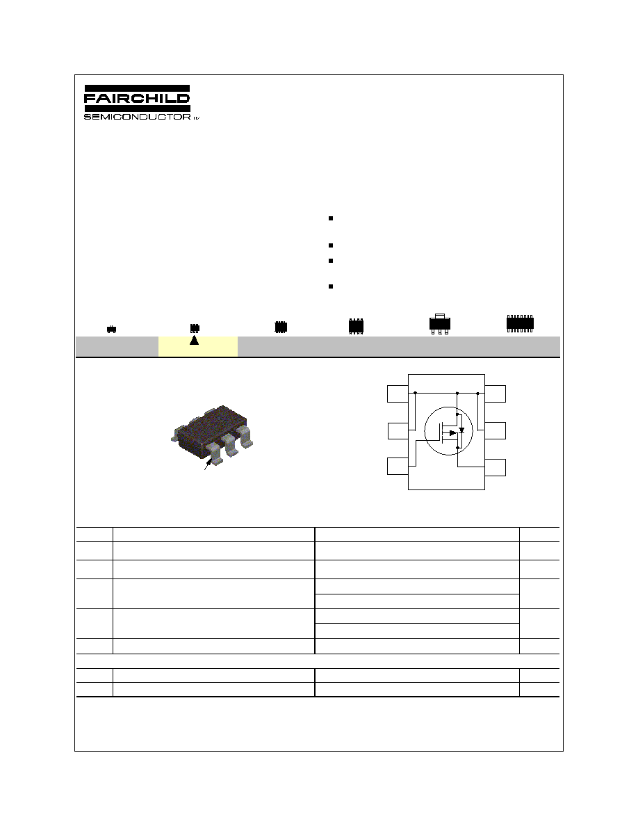
This P-Channel Logic Level MOSFET is produced
using Fairchild Semiconductor's advanced
PowerTrench process that has been especially tailored
to minimize the on-state resistance and yet maintain
low gate charge for superior switching performance.
These devices are well suited for notebook computer
applications: load switching and power management,
battery charging circuits, and DC/DC conversion.
-4 A, -30 V. R
DS(ON)
= 0.050
@ V
GS
= -10 V
R
DS(ON)
= 0.075
@ V
GS
= -4.5 V.
Low gate charge (8nC typical).
High performance trench technology for extremely low
R
DS(ON)
.
SuperSOT
TM
-6 package: small footprint (72% smaller than
standard SO-8); low profile (1mm thick).
SOIC-16
SOT-23
SuperSOT
TM
-8
SO-8
SOT-223
SuperSOT
TM
-6
D
D
D
S
D
G
SuperSOT -6
TM
.658
pin
1
3
5
6
4
1
2
3
© 1999 Fairchild Semiconductor Corporation

ELECTRICAL CHARACTERISTICS
(T
A
= 25∞C unless otherwise noted)
Symbol
Parameter
Conditions
Min
Typ
Max
Units
OFF CHARACTERISTICS
BV
DSS
Drain-Source Breakdown Voltage
V
GS
= 0 V, I
D
= -250 µA
-30
V
BV
DSS
/
T
J
Breakdown Voltage Temp. Coefficient
I
D
= -250 µA, Referenced to 25
o
C
-22
mV/
o
C
I
DSS
Zero Gate Voltage Drain Current
V
DS
= -24 V, V
GS
= 0 V
-1
µA
T
J
= 55
o
C
-10
µA
I
GSSF
Gate - Body Leakage, Forward
V
GS
= 20 V, V
DS
= 0 V
100
nA
I
GSSR
Gate - Body Leakage, Reverse
V
GS
= -20 V, V
DS
= 0 V
-100
nA
ON CHARACTERISTICS
(Note 2)
V
GS(th)
Gate Threshold Voltage
V
DS
= V
GS
, I
D
= -250 µA
-1
-1.7
-3
V
V
GS(th)
/
T
J
Gate Threshold VoltageTemp.Coefficient
I
D
= -250 µA, Referenced to 25
o
C
4.1
mV/
o
C
R
DS(ON)
Static Drain-Source On-Resistance
V
GS
= -10 V, I
D
= -4.0 A
0.041
0.05
T
J
= 125
o
C
0.058
0.08
V
GS
= -4.5 V, I
D
= -3.4 A
0.06
0.075
I
D(on)
On-State Drain Current
V
GS
= -10 V, V
DS
= -5 V
-20
A
g
FS
Forward Transconductance
V
DS
= -5V, I
D
= -4 A
9
S
DYNAMIC CHARACTERISTICS
C
iss
Input Capacitance
V
DS
= -15 V, V
GS
= 0 V,
750
pF
C
oss
Output Capacitance
f = 1.0 MHz
220
pF
C
rss
Reverse Transfer Capacitance
100
pF
SWITCHING CHARACTERISTICS
(Note 2)
t
D(on)
Turn - On Delay Time
V
DD
= -15 V, I
D
= -1 A,
12
22
ns
t
r
Turn - On Rise Time
V
GS
= -10 V, R
GEN
= 6
14
25
ns
t
D(off)
Turn - Off Delay Time
24
38
ns
t
f
Turn - Off Fall Time
16
27
ns
Q
g
Total Gate Charge
V
DS
= -15 V, I
D
= -4.0 A,
8
12
nC
Q
gs
Gate-Source Charge
V
GS
= -5 V
1.8
nC
Q
gd
Gate-Drain Charge
3
nC
DRAIN-SOURCE DIODE CHARACTERISTICS
I
S
Continuous Source Diode Current
-1.3
A
V
SD
Drain-Source Diode Forward Voltage
V
GS
= 0 V, I
S
= -1.3 A
(Note 2)
-0.76
-1.2
V
Notes:
1. R
JA
is the sum of the junction-to-case and case-to-ambient thermal resistance where the case thermal reference is defined as the solder mounting surface of the drain pins. R
JC
is guaranteed
by design while R
CA
is determined by the user's board design.
a. 78
o
C/W when mounted on a 1 in
2
pad of 2oz Cu on FR-4 board.
b. 156
o
C/W when mounted on a minimum pad of 2oz Cu on FR-4 board.
2. Pulse Test: Pulse Width < 300µs, Duty Cycle < 2.0%.
FDC658P Rev.C
FDC658P Rev.C
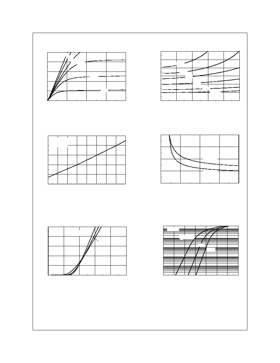
0
1
2
3
4
0
4
8
12
16
20
-V , DRAIN-SOURCE VOLTAGE (V)
- I , DRAIN-SOURCE CURRENT (A)
DS
D
-4.5V
-4.0V
-6.0V
-3.5V
-3.0V
V = -10V
GS
0
4
8
12
16
20
0.8
1
1.2
1.4
1.6
1.8
2
- I , DRAIN CURRENT (A)
DRAIN-SOURCE ON-RESISTANCE
V = -4.0 V
GS
D
R , NORMALIZED
DS(on)
-10.0V
-4.5V
-6.0V
-8.0V
-5.0V
Typical Electrical Characteristics
Figure 1. On-Region Characteristics.
Figure 2. On-Resistance Variation with
Drain Current and Gate Voltage.
Figure 3. On-Resistance Variation
with Temperature.
Figure 5. Transfer Characteristics.
0
0.2
0.4
0.6
0.8
1
1.2
1.4
0.0001
0.001
0.01
0.1
1
10
20
-V , BODY DIODE FORWARD VOLTAGE (V)
-I , REVERSE DRAIN CURRENT (A)
25∞C
-55∞C
V = 0V
GS
SD
S
T = 125∞C
J
Figure 4. On-Resistance Variation with
Gate-to-Source Voltage.
-50
-25
0
25
50
75
100
125
150
0.6
0.8
1
1.2
1.4
1.6
T , JUNCTION TEMPERATURE (∞C)
DRAIN-SOURCE ON-RESISTANCE
J
R , NORMALIZED
DS(ON)
V = -10V
GS
I = -4A
D
2
4
6
8
10
0
0.04
0.08
0.12
0.16
-V , GATE TO SOURCE VOLTAGE (V)
GS
R , ON-RESISTANCE (OHM)
DS(ON)
I = -2A
D
T = 125∞C
J
T = 25∞C
J
1
2
3
4
5
6
0
4
8
12
16
20
-V , GATE TO SOURCE VOLTAGE (V)
- I , DRAIN CURRENT (A)
V = -5V
DS
GS
D
T = -55∞C
J
125∞C
25∞C
Figure 6. Body Diode Forward Voltage
Variation with Source Current
and Temperature.
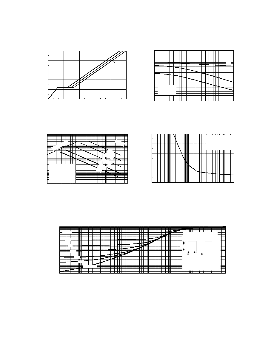
FDC658P Rev.C
Figure 10. Single Pulse Maximum Power
Dissipation.
0.1
0.3
1
3
7
15
30
30
100
300
1000
3000
-V , DRAIN TO SOURCE VOLTAGE (V)
CAPACITANCE (pF)
DS
C
iss
f = 1 MHz
V = 0 V
GS
C
oss
C
rss
Figure 8. Capacitance Characteristics
.
Figure 7. Gate Charge Characteristics.
Figure 9. Maximum Safe Operating Area.
Typical Electrical Characteristics
(continued)
0
3
6
9
12
15
0
2
4
6
8
10
Q , GATE CHARGE (nC)
-V , GATE-SOURCE VOLTAGE (V)
g
GS
V = -5V
DS
-15V
I = -4A
D
-10V
0.1
0.2
0.5
1
2
5
10
20
50
0.01
0.03
0.1
0.3
1
3
10
30
80
-V , DRAIN-SOURCE VOLTAGE (V)
-I , DRAIN CURRENT (A)
RDS(ON) LIMIT
D
DS
V = -10V
SINGLE PULSE
R = 156∞C/W
T = 25∞C
JA
GS
A
DC
1s
100ms
10ms
1ms
100us
0.01
0.1
1
10
100
300
0
1
2
3
4
5
SINGLE PULSE TIME (SEC)
POWER (W)
SINGLE PULSE
R =156∞C/W
T = 25∞C
JA
A
0.00001
0.0001
0.001
0.01
0.1
1
10
100
300
0.005
0.01
0.02
0.05
0.1
0.2
0.5
1
t , TIME (sec)
TRANSIENT THERMAL RESISTANCE
r(t), NORMALIZED EFFECTIVE
1
Single Pulse
D = 0.5
0.1
0.05
0.02
0.01
0.2
Duty Cycle, D = t / t
1
2
R (t) = r(t) * R
R = 156∞C/W
T - T = P * R (t)
A
J
P(pk)
t
1
t
2
JA
JA
JA
JA
Figure 11. Transient Thermal Response Curve.
Thermal characterization performed using the conditions described in Note 1b.
Transient thermal response will change depending on the circuit board design.

©
1998 Fairchild Semiconductor Corporation
SSOT-6 Unit Orientation
Conductive Embossed
Carrier Tape
F63TNR
Label
Customize Label
Antistatic Cover Tape
SSOT-6 Packaging
Configuration: Figure 1.0
Components
Leader Tape
390mm minimum
Trailer Tape
160mm minimum
SSOT-6 Tape Leader
Trailer
Configuration: Figure 2.0
Cover Tape
Carrier
Pin 1
Tape
Note/Comments
Packaging Option
SSOT-6 Packaging Information
Standard
(no flow code)
D87Z
Packaging type
Reel Size
TNR
7" Dia
TNR
13"
Qty per Reel/Tube/Bag
3,000
10,000
Box Dimension (mm)
184x187x47
343x343x64
Max qty per Box
9,000
20,000
Weight per unit (gm)
0.0158
0.0158
Weight per Reel (kg)
0.1440
0.4700
184mm x 184mm x 47mm
Pizza Box for Standard Option
F63TNR
Label
F63TNR Label
F63TNR Label sample
343mm x 342mm x 64mm
Intermediate box for D87Z Option
631
631
631
631
LOT: CBVK741B019
FSID: FDC633N
D/C1: D9842
QTY1:
SPEC REV: QARV:
SPEC:
QTY: 3000
D/C2:
QTY2:
CPN:
(F63TNR)2
F63TNR
Label
SuperSOT
TM
-6 Tape and Reel Data and Package Dimensions
December 1998, Rev. B