 | ÐлекÑÑоннÑй компоненÑ: FDD5680 | СкаÑаÑÑ:  PDF PDF  ZIP ZIP |
Äîêóìåíòàöèÿ è îïèñàíèÿ www.docs.chipfind.ru
FDD5680
FDD5680, Rev. C
FDD5680
N-Channel, PowerTrench
MOSFET
General Description
This N-Channel MOSFET is produced using Fairchild
Semiconductor's advanced PowerTrench process that has
been especially tailored to minimize the on-state
resistance and yet maintain low gate charge for superior
switching performance.
Applications
·
DC/DC converter
·
Motor drives
July 2000
Features
·
38 A, 60 V. R
DS(on)
= 0.021
@ V
GS
= 10 V
R
DS(on)
= 0.025
@ V
GS
= 6 V.
·
Low gate charge (33nC typical).
·
Fast switching speed.
·
High performance trench technology for extremely
low R
DS(on)
.
2000 Fairchild Semiconductor International
Absolute Maximum Ratings
T
A
=25
o
C unless otherwise noted
Symbol
Parameter
Ratings
Units
V
DSS
Drain-Source Voltage
60
V
V
GSS
Gate-Source Voltage
±
20
V
I
D
Maximun Drain Current - Continuous
(Note 1)
38
(Note 1a)
8.5
Maximum Drain Current
- Pulsed
100
A
Maximum Power Dissipation @ T
C
= 25
o
C
(Note 1)
60
T
A
= 25
o
C
(Note 1a)
2.8
P
D
T
A
= 25
o
C
(Note 1b)
1.3
W
T
J
, T
stg
Operating and Storage Junction Temperature Range
-55 to +150
°
C
Thermal Characteristics
R
JC
Thermal Resistance, Junction-to- Case
(Note 1)
2.1
°
C/W
R
JA
Thermal Resistance, Junction-to- Ambient
(Note 1b)
96
°
C/W
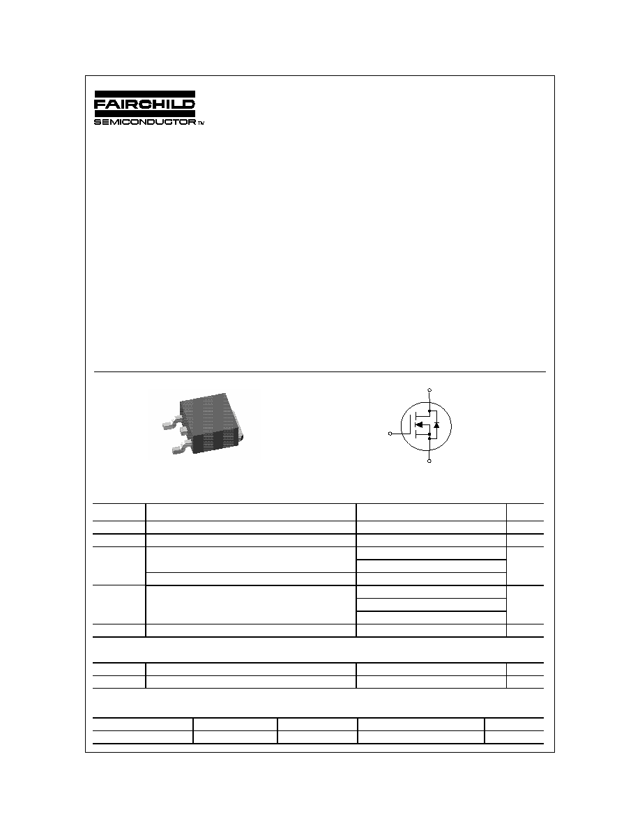
Package Marking and Ordering Information
Device Marking
Device
Reel Size
Tape width
Quantity
FDD5680
FDD5680
13''
16mm
2500
G
S
D
TO-252
S
D
G
FDD5680
FDD5680, Rev. C
Electrical Characteristics
T
A
= 25°C unless otherwise noted
Symbol
Parameter
Test Conditions
Min
Typ
Max Units
Off Characteristics
W
DSS
Single Pulse Drain-Source
Avalanche Energy
V
DD
= 30 V, I
D
= 38 A
140
mJ
I
AR
Maximum Drain-Source Avalanche Current
38
A
BV
DSS
Drain-Source Breakdown
Voltage
V
GS
= 0 V, I
D
= 250
µ
A
60
V
BV
DSS
T
J
Breakdown Voltage
Temperature Coefficient
I
D
= 250
µ
A, Referenced to 25
°
C
60
mV/
°
C
I
DSS
Zero Gate Voltage Drain Current V
DS
= 48 V, V
GS
= 0 V
1
µ
A
I
GSSF
Gate-Body Leakage Current,
Forward
V
GS
= 20V, V
DS
= 0 V
100
nA
I
GSSR
Gate-Body Leakage Current,
Reverse
V
GS
= -20 V, V
DS
= 0 V
-100
nA
On Characteristics
(Note 2)
V
GS(th)
Gate Threshold Voltage
V
DS
= V
GS
, I
D
= 250
µ
A
2
2.4
4
V
V
GS(th)
T
J
Gate Threshold Voltage
Temperature Coefficient
I
D
= 250
µ
A,Referenced to 25
°
C
-6.4
mV/
°
C
R
DS(on)
Static Drain-Source
On-Resistance
V
GS
= 10 V, I
D
= 8.5 A
V
GS
= 10 V, I
D
= 8.5 A,T
J
=125
°
C
V
GS
= 6 V, I
D
= 7.5 A
0.017
0.028
0.019
0.021
0.042
0.025
I
D(on)
On-State Drain Current
V
GS
= 10 V, V
DS
= 5 V
50
A
g
FS
Forward Transconductance
V
DS
= 5 V, I
D
= 8.5 A
30
S
Dynamic Characteristics
C
iss
Input Capacitance
1835
pF
C
oss
Output Capacitance
210
pF
C
rss
Reverse Transfer Capacitance
V
DS
= 30 V, V
GS
= 0 V,
f = 1.0 MHz
90
pF
Switching Characteristics
(Note 2)
t
d(on)
Turn-On Delay Time
15
27
ns
t
r
Turn-On Rise Time
9
18
ns
t
d(off)
Turn-Off Delay Time
35
56
ns
t
f
Turn-Off Fall Time
V
DD
= 30 V, I
D
= 1 A,
V
GS
= 10 V, R
GEN
= 6
16
26
ns
Q
g
Total Gate Charge
33
46
nC
Q
gs
Gate-Source Charge
6.5
nC
Q
gd
Gate-Drain Charge
V
DS
= 30 V, I
D
= 8.5 A,
V
GS
= 10 V,
7.5
nC
Drain-Source Diode Characteristics and Maximum Ratings
I
S
Maximum Continuous Drain-Source Diode Forward Current
2.3
A
V
SD
Drain-Source Diode Forward
Voltage
V
GS
= 0 V, I
S
= 2.3 A
(Note 2)
0.75
1.2
V
Notes:
1. R
JA
is the sum of the junction-to-case and case-to-ambient resistance where the case thermal reference is defined as the drain tab.
R
JC
is guaranteed by design while R
JA
is determined by the user's board design.
Scale 1 : 1 on letter size paper
2. Pulse Test: Pulse Width
300
µ
s, Duty Cycle
2.0%
a) R
JA
= 45oC/W when mounted
on a 1in2 pad of 2oz copper.
b) R
JA
= 96oC/W when mounted
on a 0.076 pad of 2oz copper.
FDD5680
FDD5680, Rev. C
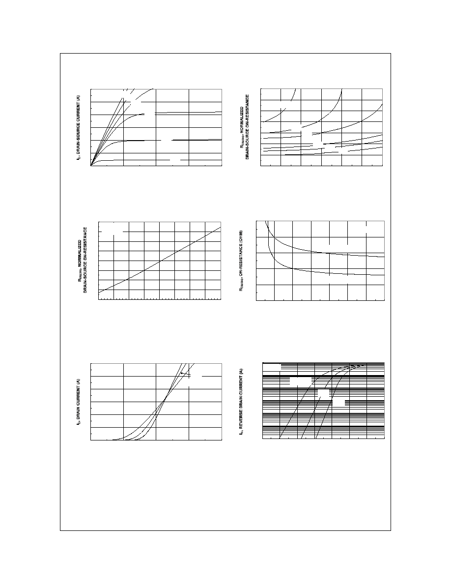
Typical Characteristics
Figure 1. On-Region Characteristics.
Figure 2. On-Resistance Variation
with Drain Current and Gate Voltage.
Figure 3. On-Resistance Variation
with Temperature.
Figure 4. On-Resistance Variation
with Gate-to-Source Voltage.
Figure 5. Transfer Characteristics.
Figure 6. Body Diode Forward Voltage
Variation with Source Current
and Temperature.
0
10
20
30
40
50
60
0
1
2
3
4
V
DS
, DRAIN-SOURCE VOLTAGE (V)
V
GS
= 10V
4.0V
5.0V
4.5V
3.5V
6.0V
0.8
1
1.2
1.4
1.6
1.8
2
2.2
0
10
20
30
40
50
60
I
D
, DRAIN CURRENT (A)
V
GS
= 4.0V
10V
5.0V
7.0V
4.5V
6.0V
0.4
0.6
0.8
1
1.2
1.4
1.6
1.8
2
-50
-25
0
25
50
75
100
125
150
T
J
, JUNCTION TEMPERATURE (
o
C)
I
D
= 8.5A
V
GS
= 10V
0
0.01
0.02
0.03
0.04
0.05
3
4
5
6
7
8
9
10
V
GS
, GATE TO SOURCE VOLTAGE (V)
I
D
= 4.3A
T
A
= 125
o
C
T
A
= 25
o
C
0
10
20
30
40
50
60
2
3
4
5
6
V
GS
, GATE TO SOURCE VOLTAGE (V)
T
A
= -55
o
C
25
o
C
125
o
C
V
DS
= 5V
0.0001
0.001
0.01
0.1
1
10
100
0
0.2
0.4
0.6
0.8
1
1.2
1.4
V
SD
, BODY DIODE FORWARD VOLTAGE (V)
T
A
= 125
o
C
25
o
C
-55
o
C
V
GS
= 0V
FDD5680
FDD5680, Rev. C
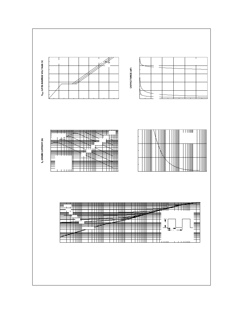
Typical Characteristics
(continued)
Figure 7. Gate-Charge Characteristics.
Figure 8. Capacitance Characteristics.
0.0001
0.001
0.01
0.1
1
10
100
300
0.0001
0.001
0.01
0.1
1
t , TIME (sec)
TR
AN
S
I
E
N
T
T
H
E
R
M
A
L
R
E
S
I
S
T
A
NCE
1
Single Pulse
D = 0.5
0.1
0.05
0.02
0.01
0.2
r
(
t
)
,
NO
R
M
AL
I
Z
E
D
E
F
F
E
CT
I
V
E
Duty Cycle, D = t / t
1
2
R (t) = r(t) * R
R =
96°C/W
JA
JA
JA
T - T = P * R (t)
JA
A
J
P(pk)
t
1
t
2
0
2
4
6
8
10
0
5
10
15
20
25
30
35
Q
g
, GATE CHARGE (nC)
I
D
= 8.5A
V
DS
= 10V
20V
30V
0
500
1000
1500
2000
2500
0
10
20
30
40
50
60
V
DS
, DRAIN TO SOURCE VOLTAGE (V)
C
ISS
C
RSS
C
OSS
f = 1MHz
V
GS
= 0 V
0.01
0.1
1
10
100
0.1
1
10
100
V
DS
, DRAIN-SOURCE VOLTAGE (V)
R
DS(ON)
LIMIT
V
GS
= 10V
SINGLE PULSE
R
JA
= 96
o
C/W
T
A
= 25
o
C
DC
10S
1S
100ms
10ms
1ms
100
µ
s
0
20
40
60
0.01
0.1
1
10
100
1000
SINGLE PULSE TIME (SEC)
PO
W
E
R
(
W
)
SINGLE PULSE
R
JA
= 96
o
C/W
T
A
= 25
o
C
Figure 9. Maximum Safe Operating Area.
Figure 10. Single Pulse Maximum
Power Dissipation.
Figure 11. Transient Thermal Response Curve.
Thermal characterization performed using the conditions described in Note 1b.
Transient themal response will change depending on the circuit board design.