 | –≠–ª–µ–∫—Ç—Ä–æ–Ω–Ω—ã–π –∫–æ–º–ø–æ–Ω–µ–Ω—Ç: FDFS2P103 | –°–∫–∞—á–∞—Ç—å:  PDF PDF  ZIP ZIP |
September 2001
2001 Fairchild Semiconductor Corporation
FDFS2P103 Rev C(W)
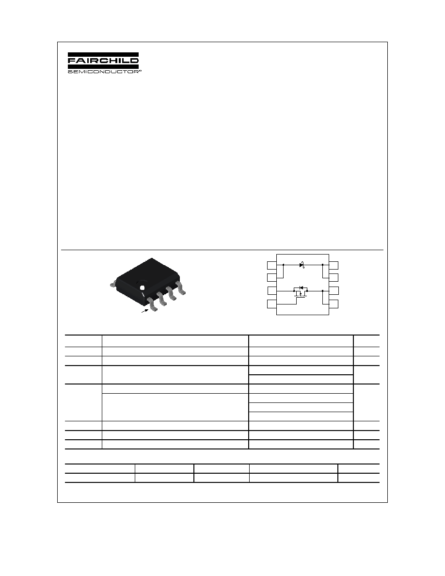
FDFS2P103
Integrated P-Channel PowerTrench
MOSFET and Schottky Diode
General Description
The FDFS2P103 combines the exceptional
performance of Fairchild's PowerTrench MOSFET
technology with a very low forward voltage drop
Schottky barrier rectifier in an SO-8 package.
This device is designed specifically as a single package
solution for DC to DC converters. It features a fast
switching, low gate charge MOSFET with very low on-
state resistance. The independently connected
Schottky diode allows its use in a variety of DC/DC
converter topologies.
Features
∑
≠5.3 A, ≠30V R
DS(ON)
= 59 m
@ V
GS
= ≠10 V
R
DS(ON)
= 92 m
@ V
GS
= ≠4.5 V
∑
V
F
< 0.52 V @ 1 A (T
J
= 125
∞
C)
V
F
< 0.57 V @ 1 A (T
J
= 25
∞
C)
∑
Schottky and MOSFET incorporated into single
power surface mount SO-8 package
∑
Electrically independent Schottky and MOSFET
pinout for design flexibility
A
A
S
G
C
C
D
D
Pin 1
SO-8
8
1
7
2
6
3
5
4
A
A
S
G
C
C
D
D
Absolute Maximum Ratings
T
A
=25
o
C unless otherwise noted
Symbol Parameter
Ratings
Units
V
DSS
MOSFET Drain-Source Voltage
≠
30
V
V
GSS
MOSFET Gate-Source Voltage
±
25
V
I
D
Drain Current ≠ Continuous
(Note 1a)
≠
5.3
A
≠
Pulsed
≠
20
Power Dissipation for Dual Operation
2
Power Dissipation for Single Operation
(Note 1a)
1.6
(Note 1b)
1
P
D
(Note 1c)
0.9
W
T
J
, T
STG
Operating and Storage Junction Temperature Range
≠
55 to +150
∞
C
V
RRM
Schottky Repetitive Peak Reverse Voltage
30 V
I
O
Schottky Average Forward Current
(Note 1a)
1 A
Package Marking and Ordering Information
Device Marking
Device
Reel Size
Tape width
Quantity
FDFS2P103 FDFS2P103 13''
12mm
2500
units
FDFS2P103

FDFS2P103 Rev C(W)
Electrical Characteristics
T
A
= 25∞C unless otherwise noted
Symbol Parameter
Test
Conditions
Min
Typ
Max
Units
Off Characteristics
BV
DSS
Drain≠Source Breakdown Voltage
V
GS
= 0 V,
I
D
= ≠250
µ
A
≠30 V
BV
DSS
T
J
Breakdown Voltage Temperature
Coefficient
I
D
= ≠250
µ
A,Referenced to 25
∞
C
≠23
mV/
∞
C
I
DSS
Zero Gate Voltage Drain Current
V
DS
= ≠24 V, V
GS
= 0 V
≠1
µ
A
I
GSSF
Gate≠Body
Leakage,
Forward V
GS
= 25 V,
V
DS
= 0 V
100
nA
I
GSSR
Gate≠Body
Leakage,
Reverse V
GS
= ≠25 V, V
DS
= 0 V
≠100
nA
On Characteristics
(Note 2)
V
GS(th)
Gate Threshold Voltage
V
DS
= V
GS
,
I
D
= ≠250
µ
A
≠1 ≠1.7 ≠3 V
V
GS(th)
T
J
Gate Threshold Voltage
Temperature Coefficient
I
D
= ≠250
µ
A,Referenced to 25
∞
C
4.5
mV/
∞
C
R
DS(on)
Static
Drain≠Source
On≠Resistance
V
GS
= ≠10 V, I
D
= ≠5.3 A
V
GS
= ≠4.5 V, I
D
= ≠4 A
V
GS
=≠10 V, I
D
=≠5.3A, T
J
=125
∞
C
46
70
63
59
92
88
m
I
D(on)
On≠State Drain Current
V
GS
= ≠10 V, V
DS
= ≠5 V
≠20
A
g
FS
Forward
Transconductance V
DS
= ≠5V,
I
D
= ≠5.3 A
10
S
Dynamic Characteristics
C
iss
Input
Capacitance
528
pF
C
oss
Output
Capacitance
132
pF
C
rss
Reverse
Transfer
Capacitance
V
DS
= ≠15 V, V
GS
= 0 V,
f = 1.0 MHz
70 pF
Switching Characteristics
(Note 2)
t
d(on)
Turn≠On
Delay
Time
7
14
ns
t
r
Turn≠On Rise Time
13
24
ns
t
d(off)
Turn≠Off
Delay
Time
14
25
ns
t
f
Turn≠Off Fall Time
V
DD
= ≠15 V, I
D
= ≠1 A,
V
GS
= ≠10 V, R
GEN
= 6
9 17 ns
Q
g
Total
Gate
Charge
5.3
8
nC
Q
gs
Gate≠Source
Charge
2.2
nC
Q
gd
Gate≠Drain
Charge
V
DS
= ≠15 V, I
D
= ≠5.3 A,
V
GS
= ≠5 V
1.6 nC
Drain≠Source Diode Characteristics and Maximum Ratings
I
S
Maximum Continuous Drain≠Source Diode Forward Current
≠1.3
A
V
SD
Drain≠Source Diode Forward
Voltage
V
GS
= 0 V, I
S
= ≠1.3 A
(Note 2)
≠0.7
≠1.2
V
Schottky Diode Characteristics
I
R
Reverse
Leakage
V
R
= 30 V
T
J
= 25
∞
C
15
100
µ
A
T
J
= 125
∞
C
6 30
mA
V
F
Forward
Voltage
I
F
= 1A
T
J
= 25
∞
C
0.41
0.57 V
T
J
= 125
∞
C
0.32
0.52 V
FDFS2P103

FDFS2P103 Rev C(W)
Thermal Characteristics
R
JA
Thermal Resistance, Junction-to-Ambient
(Note 1a)
78
∞
C/W
R
JA
Thermal Resistance, Junction-to-Ambient
(Note 1c)
135
∞
C/W
R
JC
Thermal Resistance, Junction-to-Case
(Note 1)
40
∞
C/W
Notes:
1. R
JA
is the sum of the junction-to-case and case-to-ambient thermal resistance where the case thermal reference is defined as the solder mounting surface of
the drain pins. R
JC
is guaranteed by design while R
CA
is determined by the user's board design.
a) 78∞C/W
when
mounted on a
0.5in
2
pad of 2
oz copper
b) 125∞C/W
when
mounted on a
0.02 in
2
pad of
2 oz copper
c) 135∞C/W
when
mounted on a
minimum pad.
Scale 1 : 1 on letter size paper
2. Pulse Test: Pulse Width < 300
µ
s, Duty Cycle < 2.0%
FDFS2P103
FDFS2P103 Rev C(W)
Typical Characteristics
0
10
20
30
0
1
2
3
4
5
6
-V
DS
, DRAIN TO SOURCE VOLTAGE (V)
-I
D
,
DRAI
N CURRE
NT
(A)
V
GS
= -10V
-3.0V
-3.5V
-4.0V
-4.5V
-5.0V
-6.0V
0.8
1
1.2
1.4
1.6
1.8
2
0
6
12
18
24
30
-I
D
, DRAIN CURRENT (A)
R
DS
(
O
N)
, NO
RMALIZE
D
DRAIN-
S
O
URCE
O
N
-
R
E
S
IS
TANC
E
V
GS
=-4.0V
-4.5V
-6.0V
-7.0V
-8.0V
-10V
-5.0V
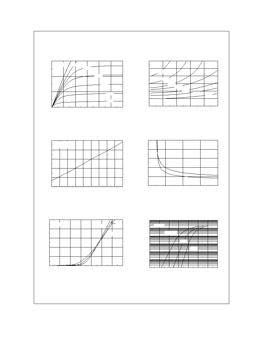
Figure 1. On-Region Characteristics.
Figure 2. On-Resistance Variation with
Drain Current and Gate Voltage.
0.6
0.8
1
1.2
1.4
1.6
-50
-25
0
25
50
75
100
125
150
175
T
J
, JUNCTION TEMPERATURE (
o
C)
R
DS
(
O
N)
,
NO
RMALI
Z
E
D
DRAI
N-S
O
URCE
O
N
-RE
S
I
S
T
ANCE
I
D
= -5.3A
V
GS
= -10V
0
0.05
0.1
0.15
0.2
0.25
2
4
6
8
10
-V
GS
, GATE TO SOURCE VOLTAGE (V)
R
DS
(
O
N)
,
O
N
-RE
S
I
S
T
ANCE
(O
HM)
I
D
= -2.8A
T
A
= 125
o
C
T
A
= 25
o
C
Figure 3. On-Resistance Variation with
Temperature.
Figure 4. On-Resistance Variation with
Gate-to-Source Voltage.
0
3
6
9
12
15
1
1.5
2
2.5
3
3.5
4
4.5
-V
GS
, GATE TO SOURCE VOLTAGE (V)
-I
D
, DRAIN CURRE
NT (
A
)
T
A
= -55
o
C
25
o
C
125
o
C
V
DS
= -5V
0.0001
0.001
0.01
0.1
1
10
100
0
0.2
0.4
0.6
0.8
1
1.2
1.4
-V
SD
,
BODY DIODE FORWARD VOLTAGE (V)
-I
S
, R
EVER
SE D
R
A
IN
C
U
R
R
E
N
T
(
A
)
V
GS
=0 V
T
A
= 125
o
C
25
o
C
-55
o
C
Figure 5. Transfer Characteristics.
Figure 6. Body Diode Forward Voltage Variation
with Source Current and Temperature.
FDFS2P103
FDFS2P103 Rev C(W)
Typical Characteristics
0
2
4
6
8
10
0
2
4
6
8
10
Q
g
, GATE CHARGE (nC)
-V
GS
,
G
A
TE
-S
O
URCE
V
O
LTAG
E
(V
)
I
D
= -5.3A
V
DS
= -10V
-15V
-20V
0
100
200
300
400
500
600
700
800
0
5
10
15
20
25
30
-V
DS
, DRAIN TO SOURCE VOLTAGE (V)
CAP
ACITANCE
(
pF)
C
ISS
C
OSS
C
RSS
f = 1 MHz
V
GS
= 0 V
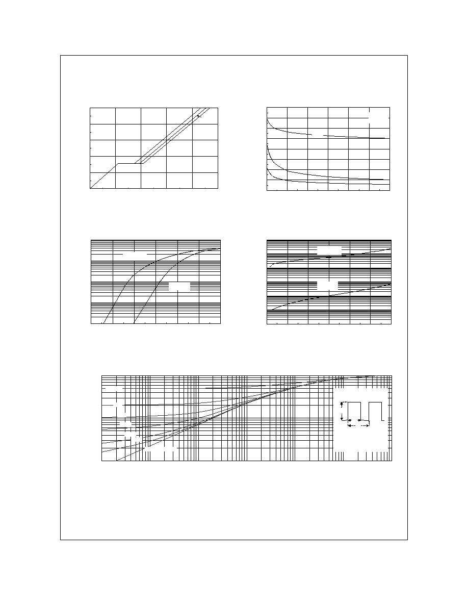
Figure 7. Gate Charge Characteristics.
Figure 8. Capacitance Characteristics.
0.001
0.01
0.1
1
10
0
0.1
0.2
0.3
0.4
0.5
0.6
V
F
, FORWARD VOLTAGE (V)
I
F
,
FO
RW
ARD LE
AKAG
E
CURRE
NT (A)
T
J
= 25
o
C
T
J
= 125
o
C
1.00E-07
1.00E-06
1.00E-05
1.00E-04
1.00E-03
1.00E-02
1.00E-01
0
10
20
30
40
50
60
V
R
, REVERSE VOLTAGE (V)
I
R
,
RE
V
E
RS
E
LE
AKAG
E
CURRE
NT (A)
T
J
= 25
o
C
T
J
= 125
o
C
Figure 9. Schottky Diode Forward Voltage.
Figure 10. Schottky Diode Reverse Current.
0.01
0.1
1
0.001
0.01
0.1
1
10
100
1000
t
1
, TIME (sec)
r
(t),
N
O
R
M
A
L
I
Z
ED
EFFEC
T
I
VE
T
RANS
IE
NT
T
H
E
R
M
A
L
RE
S
I
S
T
ANCE
R
JA
(t) = r(t) * R
JA
R
JA
= 135 ∞C/W
T
J
- T
A
= P * R
JA
(t)
Duty Cycle, D = t
1
/ t
2
P(pk)
t
1
t
2
SINGLE PULSE
0.01
0.02
0.05
0.1
0.2
D = 0.5
Figure 11. Transient Thermal Response Curve.
Thermal characterization performed using the conditions described in Note 1c.
Transient thermal response will change depending on the circuit board design.
FDFS2P103
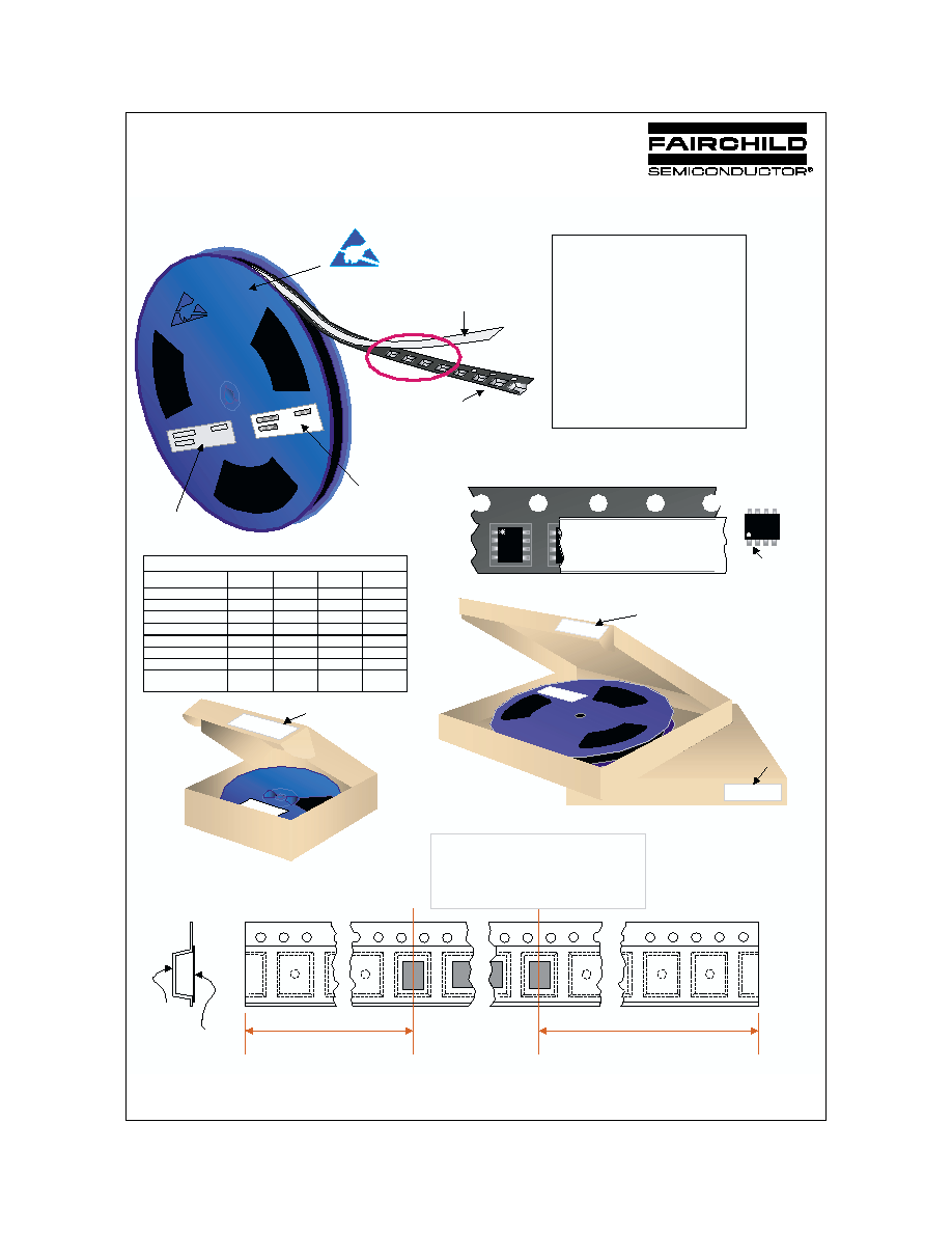
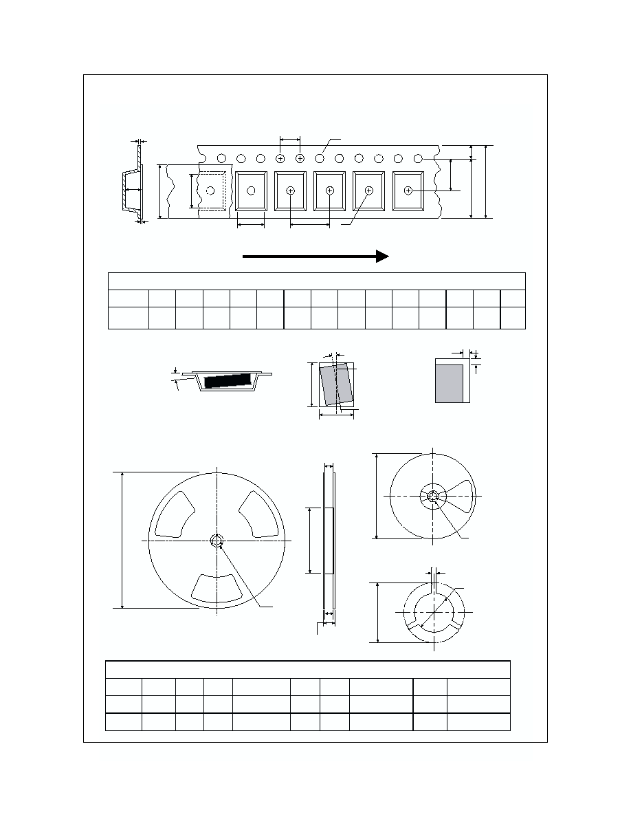
SOIC(8lds) Packag
ing
Configuration: Figure 1.0
Components
Leader Tape
1680mm minimum or
210 empty pockets
Tr ailer Ta pe
640mm minimum or
80 empty pockets
SO
IC(8lds) Tape Leader and Trailer
Configuration: Figure 2.0
Cover Tape
Carrier Tape
Note/Comments
Packaging
Option
SOIC (8lds) Packaging
Information
Standard
(no flow code)
L86Z
F011
Packaging
type
Reel Size
TNR
13" Dia
Rail/Tube
-
TNR
13" Dia
Qty per Reel/Tube/Bag
2,500
95
4,000
Box Dimension (mm)
355x333x40
530x130x83
355x333x40
Max qty per Box
5,000
30,000
8,000
D84Z
TNR
7" Dia
500
193x183x80
2,000
Weight per
unit (gm)
0.0774
0.0774
0.0774
0.0774
Weight per Reel (kg)
0.6060
-
0.9696
0.1182
Packaging Description:
SOIC-8 parts are shipped in tape. The carrier tape is
made from a dissipative (carbon filled) polycarbonate
resin. The cover tape is a multilayer film (Heat Activated
Adhesive in nature) primarily composed of polyester film,
adhesive layer, sealant, and anti-static sprayed agent.
These reeled parts in standard option are shipped with
2,500 units per 13" or 330cm diameter reel. The reels are
dark blue in color and is made of polystyrene plastic (anti-
static coated). Other option comes in 500 units per 7" or
177cm diameter reel. This and some other options are
further described in the Packaging Information table.
These full reels are individually barcode labeled and
placed inside a standard intermediate box (illustrated in
figure 1.0) made of recyclable corrugated brown paper.
One box contains two reels maximum. And these boxes
are placed inside a barcode labeled shipping box which
comes in different sizes depending on the number of parts
shipped.
F852
NDS
9959
SOIC-8 Unit Orientation
F
852
NDS
9959
Pin 1
F
852
NDS
9959
F
852
NDS
9959
F
852
NDS
9959
Barcode
Label
Barcode Label
355mm x 333mm x 40mm
Intermediate container for 13" reel option
193mm x 183mm x 80mm
Pizza Box for Standard Option
Barcode
Label
Embossed ESD Marking
AT TENTION
OBSERVE PRECAUTIONS
FOR HANDLING
ELECTROSTATIC
SENSITIVE
DEVICES
AT TENTION
OBSERVE PRECAUTIONS
FOR HANDLING
ELECTROSTATIC
SENSITIVE
DEVICES
AT TENTION
OBSERVE PRECAUTIONS
FOR HANDLING
ELECTROSTATIC
SENSITIVE
DEVICES
Static Dissipative
Embossed Carrier Tape
F63TNR
Label
Antistatic Cover Tape
Customized
Label
ATTE
NTIO
N
OBS
ERVE P
REC
AUTI
ONS
FOR
HANDLI
NG
ELE
CTR
OST
ATIC
SEN
SITI
VE
DEVI
CES
ATTE
NTIO
N
OBS
ERVE P
REC
AUTI
ONS
FOR
HANDLI
NG
ELE
CTR
OST
ATIC
SEN
SITI
VE
DEVI
CES
3000
LOT: CBVK741B019
FSID: FDS9953A
D/C1: Z9842AB
QTY1:
SPEC REV:
SPEC:
QTY: 2500
D/C2:
QTY2:
CPN:
CBVK741B019
FDS9953A
Barcode Label sample
FAIRCHILD SEMICONDUCTOR CORPORATION (F63T NR)
SOIC-8 Tape and Reel Data
June 2001, Rev. C1
©2001 Fairchild Semiconductor Corporation
„ 1998 Fairchild Semiconductor Corporation
Dimensions are in millimeter
Pkg type
A0
B0
W
D0
D1
E1
E2
F
P1
P0
K0
T
Wc
Tc
SOIC(8lds)
(12mm)
5.30
+/-0.10
6.50
+/-0.10
12.0
+/-0.3
1.55
+/-0.05
1.60
+/-0.10
1.75
+/-0.10
10.25
min
5.50
+/-0.05
8.0
+/-0.1
4.0
+/-0.1
2.1
+/-0.10
0.450
+/-
0.150
9.2
+/-0.3
0.06
+/-0.02
P1
A0
D1
P0
F
W
E1
D0
E2
B0
Tc
Wc
K0
T
Dimensions are in inches and millimeters
Tape Size
Reel
Option
Dim A
Dim B
Dim C
Dim D
Dim N
Dim W1
Dim W2
Dim W3 (LSL-USL)
12mm
7" Dia
7.00
177.8
0.059
1.5
512 +0.020/-0.008
13 +0.5/-0.2
0.795
20.2
2.165
55
0.488 +0.078/-0.000
12.4 +2/0
0.724
18.4
0.469 ≠ 0.606
11.9 ≠ 15.4
12mm
13" Dia
13.00
330
0.059
1.5
512 +0.020/-0.008
13 +0.5/-0.2
0.795
20.2
7.00
178
0.488 +0.078/-0.000
12.4 +2/0
0.724
18.4
0.469 ≠ 0.606
11.9 ≠ 15.4
See detail AA
Dim A
max
13" Diameter Option
7" Diameter Option
Dim A
Max
See detail AA
W3
W2 max Measured at Hub
W1 Measured at Hub
Dim N
Dim D
min
Dim C
B Min
DETAIL AA
Notes: A0, B0, and K0 dimensions are determined with respect to the EIA/Jedec RS-481
rotational and lateral movement requirements (see sketches A, B, and C).
20 deg maximum component rotation
0.5mm
maximum
0.5mm
maximum
Sketch C (Top View)
Component lateral movement
Typical
component
cavity
center line
20 deg maximum
Typical
component
center line
B0
A0
Sketch B (Top View)
Component Rotation
Sketch A (Side or Front Sectional View)
Component Rotation
User Direction of Feed
SOIC(8lds) Embossed Carrier Tape
Configuration: Figure 3.0
SOIC(8lds) Reel Configuration: Figure 4.0
SOIC-8 Tape and Reel Data, continued
January 2001, Rev. C

SOIC-8 (FS PKG Code S1)
1 : 1
Scale 1:1 on letter size paper
Dimensions shown below are in:
inches [millimeters]
Part Weight per unit (gram): 0.0774
SOIC-8 Package Dimensions
September 1998, Rev. A
9
©2000 Fairchild Semiconductor International

DISCLAIMER
FAIRCHILD SEMICONDUCTOR RESERVES THE RIGHT TO MAKE CHANGES WITHOUT FURTHER
NOTICE TO ANY PRODUCTS HEREIN TO IMPROVE RELIABILITY, FUNCTION OR DESIGN. FAIRCHILD
DOES NOT ASSUME ANY LIABILITY ARISING OUT OF THE APPLICATION OR USE OF ANY PRODUCT
OR CIRCUIT DESCRIBED HEREIN; NEITHER DOES IT CONVEY ANY LICENSE UNDER ITS PATENT
RIGHTS, NOR THE RIGHTS OF OTHERS.
TRADEMARKS
The following are registered and unregistered trademarks Fairchild Semiconductor owns or is authorized to use and is
not intended to be an exhaustive list of all such trademarks.
LIFE SUPPORT POLICY
FAIRCHILD'S PRODUCTS ARE NOT AUTHORIZED FOR USE AS CRITICAL COMPONENTS IN LIFE SUPPORT
DEVICES OR SYSTEMS WITHOUT THE EXPRESS WRITTEN APPROVAL OF FAIRCHILD SEMICONDUCTOR CORPORATION.
As used herein:
1. Life support devices or systems are devices or
systems which, (a) are intended for surgical implant into
the body, or (b) support or sustain life, or (c) whose
failure to perform when properly used in accordance
with instructions for use provided in the labeling, can be
reasonably expected to result in significant injury to the
user.
2. A critical component is any component of a life
support device or system whose failure to perform can
be reasonably expected to cause the failure of the life
support device or system, or to affect its safety or
effectiveness.
PRODUCT STATUS DEFINITIONS
Definition of Terms
Datasheet Identification
Product Status
Definition
Advance Information
Preliminary
No Identification Needed
Obsolete
This datasheet contains the design specifications for
product development. Specifications may change in
any manner without notice.
This datasheet contains preliminary data, and
supplementary data will be published at a later date.
Fairchild Semiconductor reserves the right to make
changes at any time without notice in order to improve
design.
This datasheet contains final specifications. Fairchild
Semiconductor reserves the right to make changes at
any time without notice in order to improve design.
This datasheet contains specifications on a product
that has been discontinued by Fairchild semiconductor.
The datasheet is printed for reference information only.
Formative or
In Design
First Production
Full Production
Not In Production
OPTOLOGICTM
OPTOPLANARTM
PACMANTM
POPTM
Power247TM
PowerTrench
QFETTM
QSTM
QT OptoelectronicsTM
Quiet SeriesTM
SILENT SWITCHER
FAST
FASTrTM
FRFETTM
GlobalOptoisolatorTM
GTOTM
HiSeCTM
ISOPLANARTM
LittleFETTM
MicroFETTM
MicroPakTM
MICROWIRETM
Rev. H4
Æ
ACExTM
BottomlessTM
CoolFETTM
CROSSVOLTTM
DenseTrenchTM
DOMETM
EcoSPARKTM
E
2
CMOS
TM
EnSigna
TM
FACTTM
FACT Quiet SeriesTM
SMART STARTTM
STAR*POWERTM
StealthTM
SuperSOTTM-3
SuperSOTTM-6
SuperSOTTM-8
SyncFETTM
TinyLogicTM
TruTranslationTM
UHCTM
UltraFET
Æ
Æ
Æ
STAR*POWER is used under license
VCXTM