 | –≠–ª–µ–∫—Ç—Ä–æ–Ω–Ω—ã–π –∫–æ–º–ø–æ–Ω–µ–Ω—Ç: FDN335N | –°–∫–∞—á–∞—Ç—å:  PDF PDF  ZIP ZIP |

FDN335N
FDN335N Rev. C
FDN335N
N-Channel 2.5V Specified PowerTrench
TM
MOSFET
General Description
This N-Channel 2.5V specified MOSFET is produced
using Fairchild Semiconductor's advanced PowerTrench
process that has been especially tailored to minimize the
on-state resistance and yet maintain low gate charge for
superior switching performance.
Applications
∑
DC/DC converter
∑
Load switch
April 1999
Features
∑
1.7 A, 20 V. R
DS(ON)
= 0.07
@ V
GS
= 4.5 V
R
DS(ON)
= 0.100
@ V
GS
= 2.5 V.
∑
Low gate charge (3.5nC typical).
∑
High performance trench technology for extremely
low R
DS(ON)
.
∑
High power and current handling capability.
©
1999 Fairchild Semiconductor Corporation
Absolute Maximum Ratings
T
A
= 25∞C unless otherwise noted
Symbol
Parameter
Ratings
Units
V
DSS
Drain-Source Voltage
20
V
V
GSS
Gate-Source Voltage
±
8
V
I
D
Drain Current
- Continuous
(Note 1a)
1.7
A
- Pulsed
8
P
D
Power Dissipation for Single Operation
(Note 1a)
0.5
W
(Note 1b)
0.46
T
J
, T
stg
Operating and Storage Junction Temperature Range
-55 to +150
∞
C
Thermal Characteristics
R
JA
Thermal Resistance, Junction-to-Ambient
(Note 1a)
250
∞
C/W
R
JC
Thermal Resistance, Junction-to-Case
(Note 1)
75
∞
C/W
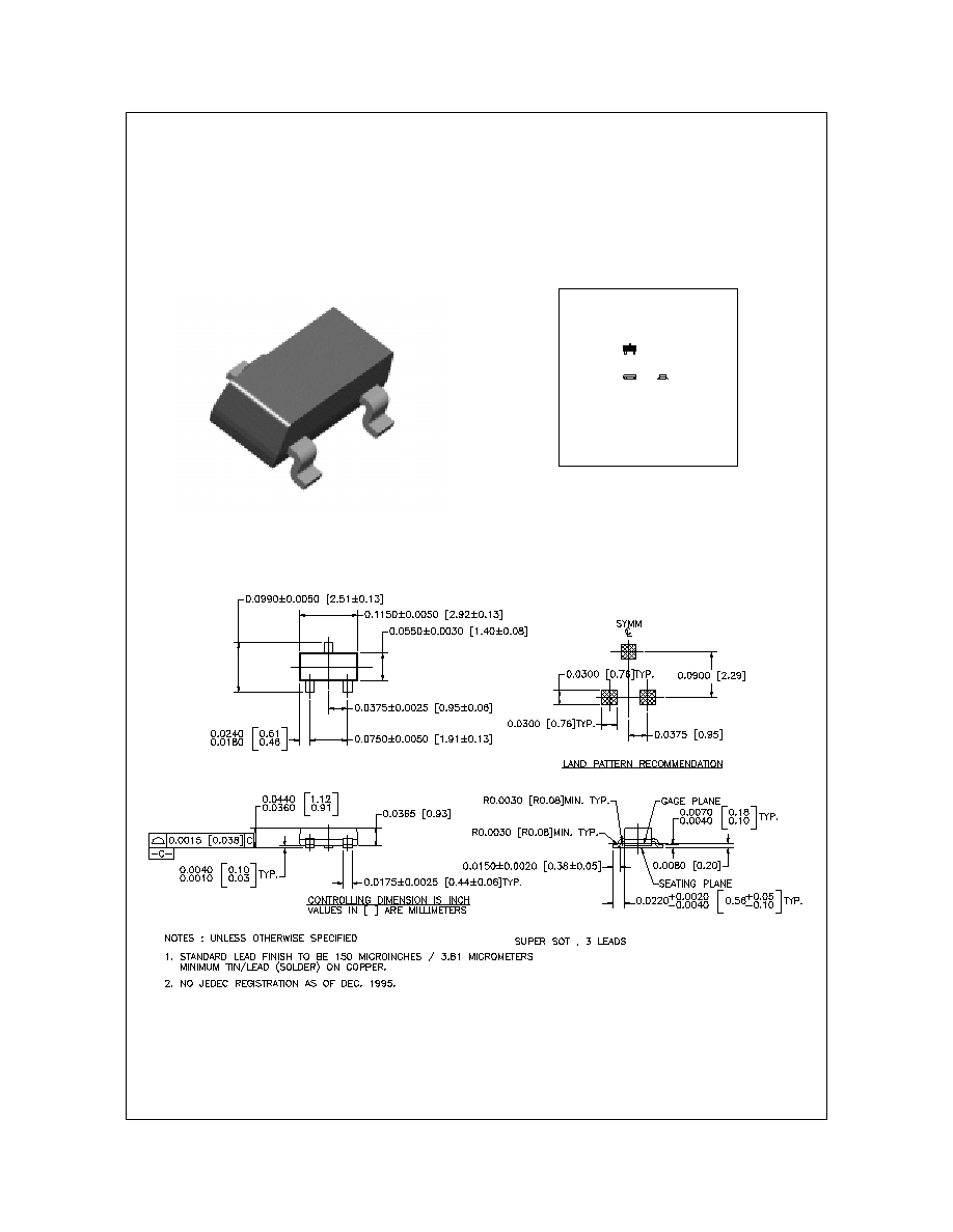
Package Outlines and Ordering Information
Device Marking
Device
Reel Size
Tape Width
Quantity
335
FDN335N
7''
8mm
3000 units
G
S
D
G
D
S
SuperSOT -3
TM

FDN335N
FDN335N Rev. C
Electrical Characteristics
T
A
= 25∞C unless otherwise noted
Symbol
Parameter
Test Conditions
Min
Typ
Max
Units
Off Characteristics
BV
DSS
Drain-Source Breakdown Voltage
V
GS
= 0 V, I
D
= 250
µ
A
20
V
BV
DSS
T
J
Breakdown Voltage Temperature
Coefficient
I
D
= 250
µ
A,Referenced to 25
∞
C
14
mV/
∞
C
I
DSS
Zero Gate Voltage Drain Current
V
DS
= 16 V, V
GS
= 0 V
1
µ
A
I
GSSF
Gate-Body Leakage Current,
Forward
V
GS
= 8 V, V
DS
= 0 V
100
nA
I
GSSR
Gate-Body Leakage Current,
Reverse
V
GS
= -8 V, V
DS
= 0 V
-100
nA
On Characteristics
(Note 2)
V
GS(th)
Gate Threshold Voltage
V
DS
= V
GS
, I
D
= 250
µ
A
0.4
0.9
1.5
V
V
GS(th)
T
J
Gate Threshold Voltage
Temperature Coefficient
I
D
= 250
µ
A,Referenced to 25
∞
C
-3
mV/
∞
C
R
DS(ON)
Static Drain-Source
On-Resistance
V
GS
= 4.5 V, I
D
= 1.7 A
V
GS
= 4.5 V, I
D
= 1.7 A,T
J
= 125
∞
C
V
GS
= 2.5 V, I
D
= 1.5 A
0.055
0.079
0.078
0.070
0.120
0.100
I
D(on)
On-State Drain Current
V
GS
= 4.5 V, V
DS
= 5 V
8
A
g
FS
Forward Transconductance
V
DS
= 5 V, I
D
= 1.5 A
7
S
Dynamic Characteristics
C
iss
Input Capacitance
310
pF
C
oss
Output Capacitance
80
pF
C
rss
Reverse Transfer Capacitance
V
DS
= 10 V, V
GS
= 0 V,
f = 1.0 MHz
40
pF
Switching Characteristics
(Note 2)
t
d(on)
Turn-On Delay Time
5
15
ns
t
r
Turn-On Rise Time
8.5
17
ns
t
d(off)
Turn-Off Delay Time
11
20
ns
t
f
Turn-Off Fall Time
V
DD
= 10 V, I
D
= 1 A,
V
GS
= 4.5 V, R
GEN
= 6
3
10
ns
Q
g
Total Gate Charge
3.5
5
nC
Q
gs
Gate-Source Charge
0.55
nC
Q
gd
Gate-Drain Charge
V
DS
= 10 V, I
D
= 1.7 A,
V
GS
= 4.5 V,
0.95
nC
Drain-Source Diode Characteristics and Maximum Ratings
I
S
Maximum Continuous Drain-Source Diode Forward Current
0.42
A
V
SD
Drain-Source Diode Forward
Voltage
V
GS
= 0 V, I
S
= 0.42 A
(Note 2)
0.7
1.2
V
Notes:
1: R
JA
is the sum of the junction-to-case and case-to-ambient thermal resistance where the case thermal reference is defined as the solder mounting
surface of the drain pins. R
JC
is guaranteed by design while R
CA
is determined by the user's board design.
Scale 1 : 1 on letter size paper
2: Pulse Test: Pulse Width
300
µ
s, Duty Cycle
2.0%
a) 250
∞
C/W when
mounted on a 0.02 in
2
Pad of 2 oz. Cu.
b) 270
∞
C/W when mounted
on a minimum pad.
FDN335N
FDN335N Rev. C
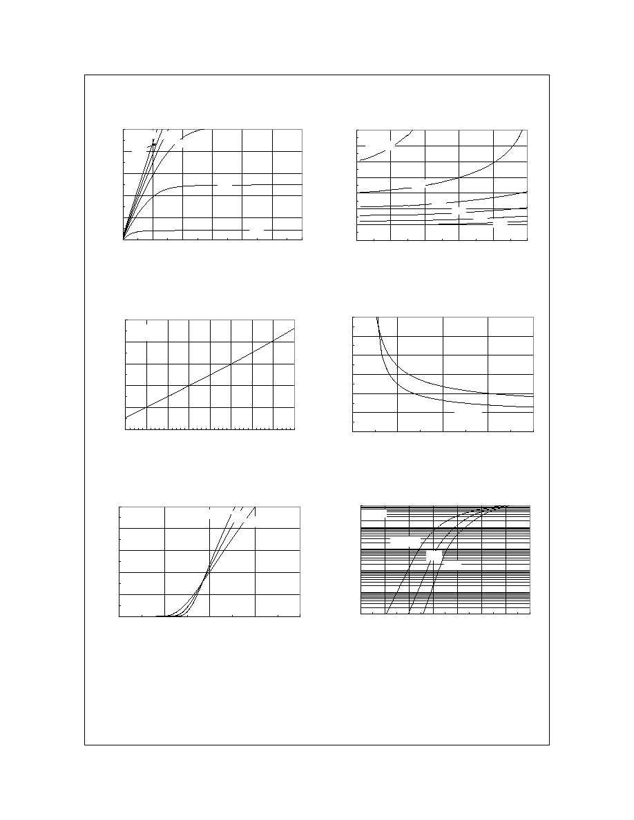
Typical Characteristics
0
2
4
6
8
10
0
1
2
3
4
V
GS
, GATE TO SOURCE VOLTAGE (V)
I
D
, DRAIN CURRENT (A)
T
A
= -55
o
C
25
o
C
125
o
C
V
DS
= 5V
0.0001
0.001
0.01
0.1
1
10
0
0.2
0.4
0.6
0.8
1
1.2
1.4
V
SD
, BODY DIODE FORWARD VOLTAGE (V)
I
S
, REVERSE DRAIN CURRENT (A)
T
A
= 125
o
C
25
o
C
-55
o
C
V
GS
= 0V
0.6
0.8
1
1.2
1.4
1.6
-50
-25
0
25
50
75
100
125
150
T
J
, JUNCTION TEMPERATURE (
o
C)
R
DS(ON)
, NORMALIZED
DRAIN-SOURCE ON-RESISTANCE
I
D
= 1.7A
V
GS
= 4.5V
0
0.04
0.08
0.12
0.16
0.2
0.24
1
2
3
4
5
V
GS
, GATE TO SOURCE VOLTAGE (V)
R
DS(ON)
, ON-RESISTANCE (OHM)
I
D
= 0.85A
T
A
= 125
o
C
T
A
= 25
o
C
0
2
4
6
8
10
0
0.5
1
1.5
2
2.5
3
V
DS
, DRAIN TO SOURCE VOLTAGE (V)
I
D
, DRAIN CURRENT (A)
V
GS
= 4.5V
3.0V
2.5V
2.0V
1.5V
3.5V
0.8
1
1.2
1.4
1.6
1.8
2
2.2
0
2
4
6
8
10
I
D
, DRAIN CURRENT (A)
R
DS(ON)
, NORMALIZED
DRAIN-SOURCE ON-RESISTANCE
V
GS
= 2.0V
2.5V
4.0V
3.5V
4.5V
3.0V
Figure 5. Transfer Characteristics.
Figure 6. Body Diode Forward Voltage
Variation with Source Current
and Temperature.
Figure 1. On-Region Characteristics.
Figure 2. On-Resistance Variation
with Drain Current and Gate Voltage.
Figure 3. On-Resistance Variation
with Temperature.
Figure 4. On-Resistance Variation
with Gate-to-Source Voltage.

FDN335N
FDN335N Rev. C
Typical Characteristics
(continued)
Figure 11. Transient Thermal Response Curve.
Thermal characterization performed using the conditions described in Note 1b.
Transient themal response will change depending on the circuit board design.
0.0001
0.001
0.01
0.1
1
10
100
300
0.001
0.002
0.005
0.01
0.02
0.05
0.1
0.2
0.5
1
t , TIME (sec)
T
R
AN
SI
E
N
T
T
H
ER
M
A
L
R
E
S
I
ST
A
N
C
E
R (t) = r(t) * R
R = 270 ∞C/W
Duty Cycle, D = t /t
1
2
JA
JA
JA
T - T = P * R (t)
JA
A
J
P(pk)
t
1
t
2
r(t
)
,
N
O
R
M
AL
I
Z
E
D
EF
F
E
C
T
I
V
E
1
Single Pulse
D = 0.5
0.1
0.05
0.02
0.01
0.2
0
4
8
12
16
20
0.0001
0.001
0.01
0.1
1
10
100
1000
SINGLE PULSE TIME (SEC)
PO
W
E
R
(
W
)
SINGLE PULSE
R
JA
=270
o
C/W
T
A
=25
o
C
0.01
0.1
1
10
0.1
1
10
100
V
DS
, DRAIN-SOURCE VOLTAGE (V)
I
D
, DRAIN CURRENT (A)
DC
10s
1s
100ms
10ms
1ms
V
GS
= 4.5V
SINGLE PULSE
R
JA
= 270
o
C/W
T
A
= 25
o
C
R
DS(ON)
LIMIT
0
1
2
3
4
5
0
0.5
1
1.5
2
2.5
3
3.5
4
Q
g
, GATE CHARGE (nC)
V
GS
, GATE-SOURCE VOLTAGE (V)
I
D
= 1.7A
V
DS
= 5V
10V
15V
0
100
200
300
400
500
0
4
8
12
16
20
V
DS
, DRAIN TO SOURCE VOLTAGE (V)
CAPACITANCE (pF)
C
ISS
C
RSS
C
OSS
f = 1MHz
V
GS
= 0 V
Figure 7. Gate Charge Characteristics.
Figure 8. Capacitance Characteristics.
Figure 9. Maximum Safe Operating Area.
Figure 10. Single Pulse Maximum
Power Dissipation.

SSOT-3 Std Unit Orientation
Conductive Embossed
Carrier Tape
Customize Label
Antistatic Cover Tape
SSOT-3 Packaging
Configuration: Figure 1.0
Components
Leader Tape
390mm minimum
Trailer Tape
160mm minimum
SSOT-23 Tape Leader and Trailer
Configuration: Figure 2.0
Cover Tape
Carrier
Pin 1
Tape
Note/Comments
Packaging Option
SSOT-3 Std Packaging Information
Standard
(no flow code)
D87Z
Packaging type
Reel Size
TNR
7" Dia
TNR
13"
Qty per Reel/Tube/Bag
3,000
10,000
Box Dimension (mm)
187x107x183
343x343x64
Max qty per Box
9,000
20,000
Weight per unit (gm)
0.0097
0.0097
Weight per Reel (kg)
0.1230
0.4150
Human Readable Label
Human Readable Label sample
343mm x 342mm x 64mm
Intermediate box for D87Z Option
Human Readable
Label
187mm x 107mm x 183mm
Intermediate Box for Standard Option
3P
3P
3P
3P
Human Readable
Label
SuperSOT
TM
-3 Tape and Reel Data and Package Dimensions
December 1998, Rev. B

Dimensions are in millimeter
Pkg type
A0
B0
W
D0
D1
E1
E2
F
P1
P0
K0
T
Wc
Tc
SSOT-3
(8mm)
3.15
+/-0.10
2.77
+/-0.10
8.0
+/-0.3
1.55
+/-0.05
1.00
+/-0.125
1.75
+/-0.10
6.25
min
3.50
+/-0.05
4.0
+/-0.1
4.0
+/-0.1
1.30
+/-0.10
0.228
+/-0.013
5.2
+/-0.3
0.06
+/-02
P1
A0
D1
P0
F
W
E1
D0
E2
B0
Tc
Wc
K0
T
Dimensions are in inches and millimeters
Tape Size
Reel
Option
Dim A
Dim B
Dim C
Dim D
Dim N
Dim W1
Dim W2
Dim W3 (LSL-USL)
8mm
7" Dia
7.00
177.8
0.059
1.5
512 +0.020/-0.008
13 +0.5/-0.2
0.795
20.2
2.165
55
0.331 +0.059/-0.000
8.4 +1.5/0
0.567
14.4
0.311 ≠ 0.429
7.9 ≠ 10.9
8mm
13" Dia
13.00
330
0.059
1.5
512 +0.020/-0.008
13 +0.5/-0.2
0.795
20.2
4.00
100
0.331 +0.059/-0.000
8.4 +1.5/0
0.567
14.4
0.311 ≠ 0.429
7.9 ≠ 10.9
See detail AA
Dim A
max
13" Diameter Option
7" Diameter Option
Dim A
Max
See detail AA
W3
W2 max Measured at Hub
W1 Measured at Hub
Dim N
Dim D
min
Dim C
B Min
DETAIL AA
Notes: A0, B0, and K0 dimensions are determined with respect to the EIA/Jedec RS-481
rotational and lateral movement requirements (see sketches A, B, and C).
20 deg maximum component rotation
0.5mm
maximum
0.5mm
maximum
Sketch C (Top View)
Component lateral movement
Typical
component
cavity
center line
20 deg maximum
Typical
component
center line
B0
A0
Sketch B (Top View)
Component Rotation
Sketch A (Side or Front Sectional View)
Component Rotation
User Direction of Feed
SSOT-3 Embossed Carrier Tape
Configuration: Figure 3.0
SSOT-3 Reel Configuration: Figure 4.0
SuperSOT
TM
-3 Tape and Reel Data and Package Dimensions, continued
December 1998, Rev. B
SuperSOT
TM
-3 (FS PKG Code 32)
1 : 1
Scale 1:1 on letter size paper
Di mensions shown below are in:
inches [mil limeters]
Part Weight per unit (gram): 0.0097
SuperSOT
TM
-3 Tape and Reel Data and Package Dimensions, continued
September 1998, Rev. A
TRADEMARKS
ACExTM
CoolFETTM
CROSSVOLTTM
E
2
CMOS
TM
FACTTM
FACT Quiet SeriesTM
FAST
Æ
FASTrTM
GTOTM
HiSeCTM
The following are registered and unregistered trademarks Fairchild Semiconductor owns or is authorized to use and is
not intended to be an exhaustive list of all such trademarks.
LIFE SUPPORT POLICY
FAIRCHILD'S PRODUCTS ARE NOT AUTHORIZED FOR USE AS CRITICAL COMPONENTS IN LIFE SUPPORT
DEVICES OR SYSTEMS WITHOUT THE EXPRESS WRITTEN APPROVAL OF FAIRCHILD SEMICONDUCTOR CORPORATION.
As used herein:
1. Life support devices or systems are devices or
systems which, (a) are intended for surgical implant into
the body, or (b) support or sustain life, or (c) whose
failure to perform when properly used in accordance
with instructions for use provided in the labeling, can be
reasonably expected to result in significant injury to the
user.
2. A critical component is any component of a life
support device or system whose failure to perform can
be reasonably expected to cause the failure of the life
support device or system, or to affect its safety or
effectiveness.
PRODUCT STATUS DEFINITIONS
Definition of Terms
Datasheet Identification
Product Status
Definition
Advance Information
Preliminary
No Identification Needed
Obsolete
This datasheet contains the design specifications for
product development. Specifications may change in
any manner without notice.
This datasheet contains preliminary data, and
supplementary data will be published at a later date.
Fairchild Semiconductor reserves the right to make
changes at any time without notice in order to improve
design.
This datasheet contains final specifications. Fairchild
Semiconductor reserves the right to make changes at
any time without notice in order to improve design.
This datasheet contains specifications on a product
that has been discontinued by Fairchild semiconductor.
The datasheet is printed for reference information only.
Formative or
In Design
First Production
Full Production
Not In Production
DISCLAIMER
FAIRCHILD SEMICONDUCTOR RESERVES THE RIGHT TO MAKE CHANGES WITHOUT FURTHER
NOTICE TO ANY PRODUCTS HEREIN TO IMPROVE RELIABILITY, FUNCTION OR DESIGN. FAIRCHILD
DOES NOT ASSUME ANY LIABILITY ARISING OUT OF THE APPLICATION OR USE OF ANY PRODUCT
OR CIRCUIT DESCRIBED HEREIN; NEITHER DOES IT CONVEY ANY LICENSE UNDER ITS PATENT
RIGHTS, NOR THE RIGHTS OF OTHERS.
SyncFETTM
TinyLogicTM
UHCTM
VCXTM
ISOPLANARTM
MICROWIRETM
POPTM
PowerTrench
QFETTM
QSTM
Quiet SeriesTM
SuperSOTTM-3
SuperSOTTM-6
SuperSOTTM-8
Rev. D