 | ÐлекÑÑоннÑй компоненÑ: FDS6681Z | СкаÑаÑÑ:  PDF PDF  ZIP ZIP |
Äîêóìåíòàöèÿ è îïèñàíèÿ www.docs.chipfind.ru
June 2005
©
2005 Fairchild Semiconductor Corporation
FDS6681Z Rev B (W)
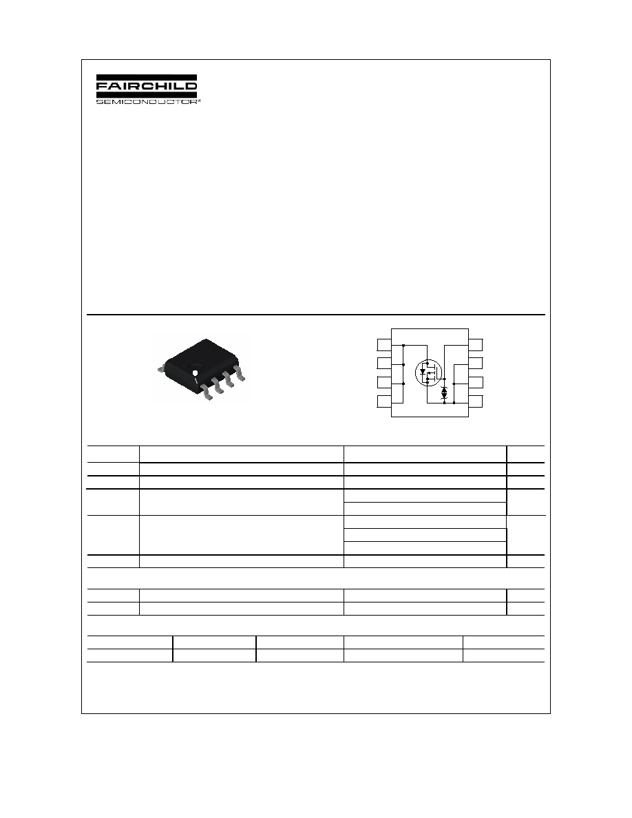
FDS6681Z
30 Volt P-Channel PowerTrench
®
MOSFET
General Description
This P-Channel MOSFET is produced using Fairchild
Semiconductor's advanced PowerTrench
®
process that
has been especially tailored to minimize the on-state
resistance.
This device is well suited for Power Management and
load switching applications common in Notebook
Computers and Portable Battery Packs.
Features
·
20 A, 30 V. R
DS(ON)
= 4.6 m
@ V
GS
= 10 V
R
DS(ON)
= 6.5 m
@ V
GS
= 4.5 V
·
Extended V
GSS
range (25V) for battery applications
·
HBM ESD protection level of 8kV typical (note 3)
·
High performance trench technology for extremely
low R
DS(ON)
·
High power and current handling capability
·
Termination is Lead-free and RoHS Compliant
S
D
S
S
SO-8
D
D
D
G
4
5
3
6
2
7
1
8
Absolute Maximum Ratings
T
A
=25
o
C unless otherwise noted
Symbol Parameter
Ratings
Units
V
DSS
Drain-Source Voltage
30
V
V
GSS
Gate-Source
Voltage
±25
V
Drain Current Continuous
(Note 1a)
20
A
I
D
Pulsed
105
P
D
Power Dissipation for Single Operation
(Note 1a)
2.5
W
(Note 1b)
1.2
(Note 1c)
1.0
T
J
, T
STG
Operating and Storage Junction Temperature Range
55 to +150
°
C
Thermal Characteristics
R
JA
Thermal Resistance, Junction-to-Ambient
(Note 1a)
50
°
C/W
R
JC
Thermal Resistance, Junction-to-Case
(Note 1)
25
°
C/W
Package Marking and Ordering Information
Device Marking
Device
Reel Size
Tape width
Quantity
FDS6681Z
FDS6681Z
13''
12mm
2500 units
FDS6681Z
FDS6681Z Rev B (W)
Electrical Characteristics
T
A
= 25°C unless otherwise noted
Symbol Parameter
Test
Conditions
Min
Typ
Max
Units
Off Characteristics
BV
DSS
DrainSource Breakdown Voltage
V
GS
= 0 V,
I
D
= 250
µ
A
30 V
BV
DSS
T
J
Breakdown Voltage Temperature
Coefficient
I
D
= 250
µ
A, Referenced to 25
°
C
26 mV/
°
C
I
DSS
Zero Gate Voltage Drain Current
V
DS
= 24 V, V
GS
= 0 V
1
µ
A
I
GSS
GateBody
Leakage
V
GS
= ±25 V, V
DS
= 0 V
±10
µ
A
On Characteristics
(Note 2)
V
GS(th)
Gate Threshold Voltage
V
DS
= V
GS
, I
D
= 250
µ
A
1 1.8 3 V
V
GS(th)
T
J
Gate Threshold Voltage
Temperature Coefficient
I
D
= 250
µ
A, Referenced to 25
°
C
6
mV/
°
C
R
DS(on)
Static DrainSource
OnResistance
V
GS
= 10 V, I
D
= 20 A
V
GS
= 4.5 V, I
D
= 17 A
V
GS
= 10 V, I
D
= 20 A,T
J
=125
°
C
3.8
5.2
5.0
4.6
6.5
6.3
m
g
FS
Forward
Transconductance V
DS
= 5 V, I
D
= 20 A
79
S
Dynamic Characteristics
C
iss
Input
Capacitance
7540
pF
C
oss
Output
Capacitance
1400
pF
C
rss
Reverse Transfer Capacitance
V
DS
= 15 V, V
GS
= 0 V,
f = 1.0 MHz
1120 pF
Switching Characteristics
(Note 2)
t
d(on)
TurnOn
Delay
Time
20
35
ns
t
r
TurnOn Rise Time
9
18
ns
t
d(off)
TurnOff Delay Time
660
1060
ns
t
f
TurnOff
Fall
Time
V
DD
= 15 V, I
D
= 1 A,
V
GS
= 10 V, R
GEN
= 6
380
610 ns
Q
g(TOT)
Total Gate Charge at V
GS
= 10V
185
260
nC
Q
g(TOT)
Total Gate Charge at V
GS
= 5V
105
150
nC
Q
gs
GateSource
Charge
26
nC
Q
gd
GateDrain
Charge
V
DS
= 15 V, I
D
= 20 A
47 nC
FDS6681Z
FDS6681Z Rev B (W)
Electrical Characteristics
T
A
= 25°C unless otherwise noted
Symbol Parameter
Test
Conditions
Min
Typ
Max
Units
DrainSource Diode Characteristics and Maximum Ratings
I
S
Maximum Continuous DrainSource Diode Forward Current
2.1
A
V
SD
DrainSource Diode Forward
Voltage
V
GS
= 0 V, I
S
= 2.1 A
(Note 2)
0.7
1.2
V
t
RR
Reverse Recovery Time
I
F
= 20 A,
125 ns
Q
RR
Reverse Recovery Charge
dI
F
/dt = 100 A/µs
(Note
2)
94
nC
Notes:
1. R
JA
is the sum of the junction-to-case and case-to-ambient thermal resistance where the case thermal reference is defined as the solder mounting surface of the
drain pins. R
JC
is guaranteed by design while R
CA
is determined by the user's board design.
a) 50°C/W (10 sec)
62.5°C/W steady state
when mounted on a
1in
2
pad of 2 oz
copper
b) 105°C/W when
mounted on a .04 in
2
pad of 2 oz copper
c) 125°C/W when mounted
on a minimum pad.
Scale 1 : 1 on letter size paper
2. Pulse Test: Pulse Width < 300
µ
s, Duty Cycle < 2.0%
3. The diode connected between the gate and source serves only as protection against ESD. No gate overvoltage rating is implied.
FDS6681Z
FDS6681Z Rev B (W)
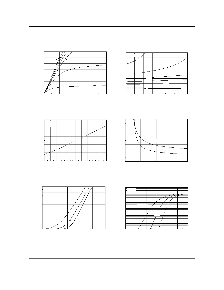
Typical Characteristics
0
15
30
45
60
75
90
105
0
0.5
1
1.5
2
-V
DS
, DRAIN-SOURCE VOLTAGE (V)
-I
D
,
DR
AI
N CU
RRE
NT
(A
)
-6.0V
-3.5V
V
GS
= -10V
-4.0V
-3.0V
-4.5V
0.8
1
1.2
1.4
1.6
1.8
2
2.2
2.4
0
15
30
45
60
75
90
105
-I
D
, DRAIN CURRENT (A)
R
DS
(O
N)
,
NO
R
M
ALI
Z
ED
D
RAI
N-
S
O
UR
CE
O
N
-
R
E
S
I
S
T
AN
CE
V
GS
= -3.5V
-4.5V
-4.0V
-8.0V
-10V
-5.0V
-6.0V
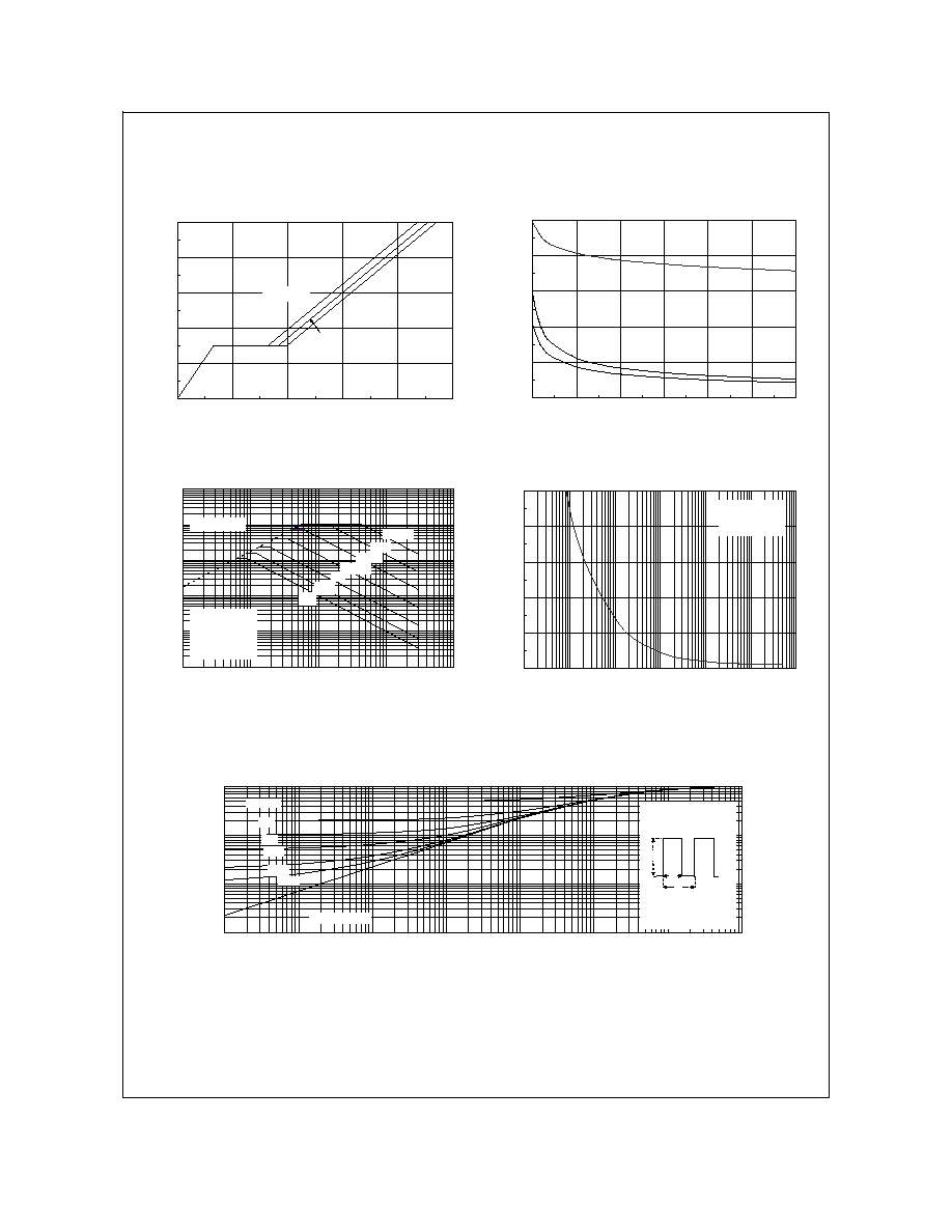
Figure 1. On-Region Characteristics.
Figure 2. On-Resistance Variation with
Drain Current and Gate Voltage.
0.6
0.8
1
1.2
1.4
1.6
-50
-30
-10
10
30
50
70
90
110
130
150
T
J
, JUNCTION TEMPERATURE (
o
C)
R
DS
(
O
N)
,
NO
RM
AL
I
Z
E
D
DR
AIN
-
SO
URC
E O
N
-
R
ESI
ST
ANC
E
I
D
= -20A
V
GS
= -10V
0.002
0.004
0.006
0.008
0.01
0.012
2
4
6
8
10
-V
GS
, GATE TO SOURCE VOLTAGE (V)
R
DS
(
O
N)
, ON
-R
ES
IS
TA
NC
E
(OH
M
)
I
D
= -10A
T
A
= 125
o
C
T
A
= 25
o
C
Figure 3. On-Resistance Variation with
Temperature.
Figure 4. On-Resistance Variation with
Gate-to-Source Voltage.
0
15
30
45
60
75
90
105
1
1.25
1.5
1.75
2
2.25
-V
GS
, GATE TO SOURCE VOLTAGE (V)
-I
D
,
D
RAI
N C
U
R
R
E
N
T
(
A
)
T
A
= 125
o
C
25
o
C
-55
o
C
V
DS
= -5V
0.001
0.01
0.1
1
10
100
1000
0
0.2
0.4
0.6
0.8
1
1.2
-V
SD
, BODY DIODE FORWARD VOLTAGE (V)
-I
S
,
R
E
V
E
RS
E DR
AI
N CU
RRE
NT
(
A
)
T
A
= 125
o
C
25
o
C
-55
o
C
V
GS
= 0V
Figure 5. Transfer Characteristics.
Figure 6. Body Diode Forward Voltage Variation
with Source Current and Temperature.
FDS6681Z
FDS6681Z Rev B (W)
Typical Characteristics
0
2
4
6
8
10
0
40
80
120
160
200
Q
g
, GATE CHARGE (nC)
-V
GS
, GA
T
E
-S
OU
RC
E V
O
LTAG
E
(
V
)
I
D
= -20A
V
DS
= -10V
-20V
-15V
0
2000
4000
6000
8000
10000
0
5
10
15
20
25
30
-V
DS
, DRAIN TO SOURCE VOLTAGE (V)
CAP
A
C
I
T
A
NCE
(
p
F
)
C
iss
C
rss
C
oss
f = 1MHz
V
GS
= 0 V
Figure 7. Gate Charge Characteristics.
Figure 8. Capacitance Characteristics.
0.01
0.1
1
10
100
1000
0.01
0.1
1
10
100
-V
DS
, DRAIN-SOURCE VOLTAGE (V)
-I
D
,
D
RAI
N CU
RR
E
N
T (A)
DC
1s
100ms
R
DS(ON)
LIMIT
V
GS
= -10V
SINGLE PULSE
R
JA
= 125
o
C/W
T
A
= 25
o
C
10ms
10s
100us
1ms
0
10
20
30
40
50
0.001
0.01
0.1
1
10
100
1000
t
1
, TIME (sec)
P
(
p
k
)
,
P
E
A
K
TR
ANS
I
E
N
T
PO
W
E
R (
W
)
SINGLE PULSE
R
JA
= 125°C/W
T
A
= 25°C
Figure 9. Maximum Safe Operating Area.
Figure 10. Single Pulse Maximum
Power Dissipation.
0.001
0.01
0.1
1
0.0001
0.001
0.01
0.1
1
10
100
1000
t
1
, TIME (sec)
r
(t)
, N
O
R
M
AL
IZ
ED
EF
F
E
CT
I
V
E T
RANS
I
E
NT
T
H
ER
M
A
L
RE
SI
S
T
AN
CE
R
JA
(t) = r(t) * R
JA
R
JA
= 125 °C/W
T
J
- T
A
= P * R
JA
(t)
Duty Cycle, D = t
1
/ t
2
P(pk
t
1
t
2
SINGLE PULSE
0.01
0.02
0.05
0.1
0.2
D = 0.5
Figure 11. Transient Thermal Response Curve.
Thermal characterization performed using the conditions described in Note 1c.
Transient thermal response will change depending on the circuit board design.
FDS6681Z

DISCLAIMER
FAIRCHILD SEMICONDUCTOR RESERVES THE RIGHT TO MAKE CHANGES WITHOUT FURTHER NOTICE TO ANY
PRODUCTS HEREIN TO IMPROVE RELIABILITY, FUNCTION OR DESIGN. FAIRCHILD DOES NOT ASSUME ANY LIABILITY
ARISING OUT OF THE APPLICATION OR USE OF ANY PRODUCT OR CIRCUIT DESCRIBED HEREIN; NEITHER DOES IT
CONVEY ANY LICENSE UNDER ITS PATENT RIGHTS, NOR THE RIGHTS OF OTHERS.
TRADEMARKS
The following are registered and unregistered trademarks Fairchild Semiconductor owns or is authorized to use and is
not intended to be an exhaustive list of all such trademarks.
LIFE SUPPORT POLICY
FAIRCHILD'S PRODUCTS ARE NOT AUTHORIZED FOR USE AS CRITICAL COMPONENTS IN LIFE SUPPORT
DEVICES OR SYSTEMS WITHOUT THE EXPRESS WRITTEN APPROVAL OF FAIRCHILD SEMICONDUCTOR CORPORATION.
As used herein:
1. Life support devices or systems are devices or
systems which, (a) are intended for surgical implant into
the body, or (b) support or sustain life, or (c) whose
failure to perform when properly used in accordance
with instructions for use provided in the labeling, can be
reasonably expected to result in significant injury to the
user.
2. A critical component is any component of a life
support device or system whose failure to perform can
be reasonably expected to cause the failure of the life
support device or system, or to affect its safety or
effectiveness.
PRODUCT STATUS DEFINITIONS
Definition of Terms
Datasheet Identification
Product Status
Definition
Advance Information
Preliminary
No Identification Needed
Obsolete
This datasheet contains the design specifications for
product development. Specifications may change in
any manner without notice.
This datasheet contains preliminary data, and
supplementary data will be published at a later date.
Fairchild Semiconductor reserves the right to make
changes at any time without notice in order to improve
design.
This datasheet contains final specifications. Fairchild
Semiconductor reserves the right to make changes at
any time without notice in order to improve design.
This datasheet contains specifications on a product
that has been discontinued by Fairchild semiconductor.
The datasheet is printed for reference information only.
Formative or
In Design
First Production
Full Production
Not In Production
ISOPLANARTM
LittleFETTM
MICROCOUPLERTM
MicroFETTM
MicroPakTM
MICROWIRETM
MSXTM
MSXProTM
OCXTM
OCXProTM
OPTOLOGIC
®
OPTOPLANARTM
PACMANTM
POPTM
Power247TM
PowerEdgeTM
FAST
®
FASTrTM
FPSTM
FRFETTM
GlobalOptoisolatorTM
GTOTM
HiSeCTM
I
2
CTM
i-LoTM
ImpliedDisconnectTM
IntelliMAXTM
Rev. I16
ACExTM
ActiveArrayTM
BottomlessTM
Build it NowTM
CoolFETTM
CROSSVOLTTM
DOMETM
EcoSPARKTM
E
2
CMOSTM
EnSignaTM
FACTTM
FACT Quiet SeriesTM
PowerSaverTM
PowerTrench
®
QFET
®
QSTM
QT OptoelectronicsTM
Quiet SeriesTM
RapidConfigureTM
RapidConnectTM
SerDesTM
SILENT SWITCHER
®
SMART STARTTM
SPMTM
StealthTM
SuperFETTM
SuperSOTTM-3
SuperSOTTM-6
SuperSOTTM-8
SyncFETTM
TinyLogic
®
TINYOPTOTM
TruTranslationTM
UHCTM
UltraFET
®
UniFETTM
VCXTM
WireTM
Across the board. Around the world.TM
The Power Franchise
®
Programmable Active DroopTM