©2003 Fairchild Semiconductor Corporation
May 2003
FF1N30HS60DD
FFH1N30HS60DD RevA
FF1N30HS60DD
30A, 600V StealthTM Diode
General Description
The FF1N30HS60DD is a StealthTM diode optimized for low
loss performance in high frequency hard switched applications.
The StealthTM family exhibits low reverse recovery current
(I
RM(REC)
) and exceptionally soft recovery under typical
operating conditions.
This device is intended for use as a free wheeling or boost
diode in power supplies and other power switching
applications. The low I
RM(REC)
and short t
a
phase reduce loss
in switching transistors. The soft recovery minimizes ringing,
expanding the range of conditions under which the diode may
be operated without the use of additional snubber circuitry.
Consider using the StealthTM diode with an SMPS IGBT to
provide the most efficient and highest power density design at
lower cost.
Formerly developmental type TA49411
.
Features
∑ Soft Recovery . . . . . . . . . . . . . . . . . . . . . . . . t
b
/ t
a
> 1.2
∑ Fast Recovery . . . . . . . . . . . . . . . . . . . . . . . . . t
rr
< 35ns
∑ Operating Temperature . . . . . . . . . . . . . . . . . . . . 175
o
C
∑ Reverse Voltage . . . . . . . . . . . . . . . . . . . . . . . . . . . 600V
∑ Fully Isolated Package (2,500 volt AC)
∑ Extremely Low Switching Losses
∑ Avalanche Energy Rated
Applications
∑ Switch Mode Power Supplies
∑ Hard Switched CCM PFC Boost Diode
∑ UPS and Motor Drive Free Wheeling Diode
∑ SMPS FWD
∑ Snubber Diode
Device Maximum Ratings
(per diode)
T
C
= 25∞C unless otherwise noted
Symbol
Parameter
Ratings
Units
V
RRM
Repetitive Peak Reverse Voltage
600
V
V
RWM
Working Peak Reverse Voltage
600
V
V
R
DC Blocking Voltage
600
V
I
F(AV)
Average Rectified Forward Current (T
C
= 110
o
C)
30
A
I
FRM
Repetitive Peak Surge Current (20kHz Square Wave)
70
A
I
FSM
Nonrepetitive Peak Surge Current (Halfwave 1 Phase 60Hz)
325
A
P
D
Power Dissipation
136
W
E
AVL
Avalanche Energy (1A, 40mH)
20
mJ
T
J
, T
STG
Operating and Storage Temperature Range
-55 to 175
∞C
M
d
Mounting force
Terminal connection torque
1.5/13
1.5/13
Nm/lb.in.
Nm/lb.in.
T
L
T
PKG
Maximum Temperature for Soldering
Leads at 0.063in (1.6mm) from Case for 10s
Package Body for 10s, See Techbrief TB334
300
260
∞C
∞C
CAUTION: Stresses above those listed in "Device Maximum Ratings" may cause permanent damage to the device. This is a stress only rating and
operation of the device at these or any other conditions above those indicated in the operational sections of this specification is not implied.
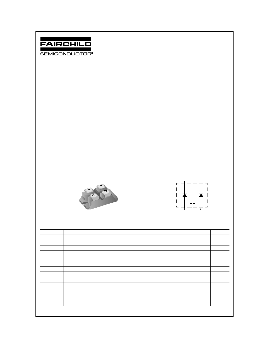
K
A
JEDEC SOT-227
K
A
Package
Symbol

©2003 Fairchild Semiconductor Corporation
FFH1N30HS60DD RevA
FF1N30HS60DD
Package Marking and Ordering Information
Electrical Characteristics
(per diode)
T
C
= 25∞C unless otherwise noted
Off State Characteristics
On State Characteristics
Dynamic Characteristics
Switching Characteristics
Thermal Characteristics
Device Marking
Device
Package
Tape Width
Quantity
FF1N30HS60DD
FF1N30HS60DD
SOT-227
-
10
Symbol
Parameter
Test Conditions
Min
Typ
Max
Units
I
R
Instantaneous Reverse Current
V
R
= 600V
T
C
= 25∞C
-
-
100
µ
A
T
C
= 125∞C
-
-
1.0
mA
V
F
Instantaneous Forward Voltage
I
F
= 30A
T
C
= 25∞C
-
2.1
2.4
V
T
C
= 125∞C
-
1.7
2.1
V
C
J
Junction Capacitance
V
R
= 10V, I
F
= 0A
-
120
-
pF
t
rr
Reverse Recovery Time
I
F
= 1A, dI
F
/dt = 100A/
µ
s, V
R
= 30V
-
27
35
ns
I
F
= 30A, dI
F
/dt = 100A/
µ
s, V
R
= 30V
-
36
45
ns
t
rr
Reverse Recovery Time
I
F
= 30A,
dI
F
/dt = 200A/
µ
s,
V
R
= 390V, T
C
= 25∞C
-
36
-
ns
I
RM(REC)
Maximum Reverse Recovery Current
-
2.9
-
A
Q
RR
Reverse Recovered Charge
-
55
-
nC
t
rr
Reverse Recovery Time
I
F
= 30A,
dI
F
/dt = 200A/
µ
s,
V
R
= 390V,
T
C
= 125∞C
-
110
-
ns
S
Softness Factor (t
b
/t
a
)
-
1.9
-
I
RM(REC)
Maximum Reverse Recovery Current
-
6
-
A
Q
RR
Reverse Recovered Charge
-
450
-
nC
t
rr
Reverse Recovery Time
I
F
= 30A,
dI
F
/dt = 1000A/
µ
s,
V
R
= 390V,
T
C
= 125∞C
-
60
-
ns
S
Softness Factor (t
b
/t
a
)
-
1.25
-
I
RM(REC)
Maximum Reverse Recovery Current
-
21
-
A
Q
RR
Reverse Recovered Charge
730
-
nC
dI
M
/dt
Maximum di/dt during t
b
-
800
-
A/µs
R
JC
Thermal Resistance Junction to Case
-
-
1.1
∞C/W
R
JA
Thermal Resistance Junction to Ambient SOT-227
-
-
12
∞C/W

©2003 Fairchild Semiconductor Corporation
FFH1N30HS60DD RevA
FF1N30HS60DD
Typical Performance Curves
Figure 1. Forward Current vs Forward Voltage
Figure 2. Reverse Current vs Reverse Voltage
Figure 3. t
a
and t
b
Curves vs Forward Current
Figure 4. t
a
and t
b
Curves vs dI
F
/dt
Figure 5. Maximum Reverse Recovery Current vs
Forward Current
Figure 6. Maximum Reverse Recovery Current vs
dI
F
/dt
V
F
, FORWARD VOLTAGE (V)
I
F
, F
O
R
W
A
RD CURRENT
(
A
)
60
50
40
0
0
1.0
2.0
3.0
30
20
10
0.5
1.5
2.5
25
o
C
175
o
C
100
o
C
150
o
C
125
o
C
10
V
R
, REVERSE VOLTAGE (V)
I
R
, REVE
RSE
C
URRENT
(
µ
A)
100
100
200
500
600
400
1000
1
0.1
175
o
C
25
o
C
100
o
C
300
5000
75
o
C
150
o
C
125
o
C
I
F
, FORWARD CURRENT (A)
0
0
20
40
60
80
100
20
60
t
,
RE
CO
VE
R
Y
TI
M
ES (
n
s
)
t
b
AT dI
F
/dt = 200A/µs, 500A/µs, 800A/µs
V
R
= 390V, T
J
= 125
o
C
10
30
40
50
t
a
AT dI
F
/dt = 200A/µs, 500A/µs, 800A/µs
90
70
50
30
10
dI
F
/dt, CURRENT RATE OF CHANGE (A/µs)
0
20
40
60
80
120
t
,
RECO
VER
Y T
I
M
E
S (
n
s
)
V
R
= 390V, T
J
= 125
o
C
t
b
AT I
F
= 60A, 30A, 15A
1000
1600
1400
400
200
600
800
1200
t
a
AT I
F
= 60A, 30A, 15A
100
I
F
, FORWARD CURRENT (A)
4
8
10
12
14
18
20
I
R
M(R
E
C
)
, M
A
X
REVE
RSE RE
CO
VE
R
Y
CURRENT
(
A
)
dI
F
/dt = 800A/µs
dI
F
/dt = 500A/µs
dI
F
/dt = 200A/µs
V
R
= 390V, T
J
= 125
o
C
0
20
60
10
30
40
50
6
16
dI
F
/dt, CURRENT RATE OF CHANGE (A/µs)
0
5
10
15
20
25
V
R
= 390V, T
J
= 125
o
C
I
F
= 60A
I
F
= 15A
I
RM
(
R
EC)
, M
A
X RE
VERS
E
RECO
VER
Y CURRE
NT
(
A
)
30
I
F
= 30A
1000
1600
1400
400
200
600
800
1200

©2003 Fairchild Semiconductor Corporation
FFH1N30HS60DD RevA
FF1N30HS60DD
Figure 7. Reverse Recovery Softness Factor vs
dI
F
/dt
Figure 8. Reverse Recovered Charge vs dI
F
/dt
Figure 9. Junction Capacitance vs Reverse
Voltage
Figure 10. DC Current Derating Curve
Figure 11. Normalized Maximum Transient Thermal Impedance
Typical Performance Curves (Continued)
dI
F
/dt, CURRENT RATE OF CHANGE (A/µs)
0.5
1.0
1.5
2.0
2.5
V
R
= 390V, T
J
= 125
o
C
I
F
= 60A
I
F
= 30A
I
F
= 15A
S, REV
E
RSE
RECO
V
E
R
Y
SOF
T
NE
SS F
A
CT
OR
1000
1600
1400
400
200
600
800
1200
2.25
1.75
1.25
0.75
dI
F
/dt, CURRENT RATE OF CHANGE (A/µs)
200
400
600
800
1000
1200
V
R
= 390V, T
J
= 125
o
C
I
F
= 60A
I
F
= 30A
I
F
= 15A
Q
RR
,
REVE
RSE
R
E
CO
V
E
RED
CH
ARGE
(
n
C)
1000
1600
1400
400
200
600
800
1200
400
0
800
600
200
1000
V
R
, REVERSE VOLTAGE (V)
C
J
, J
UNCT
ION CAP
A
C
IT
ANCE (
p
F
)
0.1
1
100
10
I
F(
A
V
)
, A
V
ERA
G
E F
O
R
W
A
RD CURRENT
(
A
)
T
C
, CASE TEMPERATURE
0
5
10
15
20
35
25
30
145
175
165
115
105
125
135
155
t, RECTANGULAR PULSE DURATION (s)
10
-5
10
-2
10
-1
Z
JA
, NORM
AL
IZ
ED
T
H
ERM
A
L
IM
PE
D
ANCE
0.01
10
-4
10
-3
10
0
0.1
10
1
1.0
SINGLE PULSE
DUTY CYCLE - DESCENDING ORDER
0.5
0.2
0.1
0.05
0.01
0.02
NOTES:
DUTY FACTOR: D = t
1
/t
2
PEAK T
J
= P
DM
x Z
JA
x R
JA
+ T
A
P
DM
t
1
t
2
2.0
0.001

©2003 Fairchild Semiconductor Corporation
FFH1N30HS60DD RevA
FF1N30HS60DD
Figure 12. t
rr
Test Circuit
Figure 13. t
rr
Waveforms and Definitions
Figure 14. Avalanche Energy Test Circuit
Figure 15. Avalanche Current and Voltage
Waveforms
Typical Performance Curves (Continued)
R
G
L
V
DD
MOSFET
CURRENT
SENSE
DUT
V
GE
t
1
t
2
V
GE
AMPLITUDE AND
t
1 AND
t
2
CONTROL I
F
R
G
CONTROL dI
F
/dt
+
-
dt
dI
F
I
F
trr
ta
tb
0
I
RM
0.25 I
RM
DUT
CURRENT
SENSE
+
L
R
V
DD
R < 0.1
E
AVL
= 1/2LI
2
[V
R(AVL)
/(V
R(AVL)
- V
DD
)]
Q
1
= IGBT (BV
CES
> DUT V
R(AVL)
)
-
V
DD
Q
1
I = 1A
L = 40mH
V
DD
= 50V
I V
t
0
t
1
t
2
I
L
V
AVL
t
I
L
Test Circuit and Waveforms