 | –≠–ª–µ–∫—Ç—Ä–æ–Ω–Ω—ã–π –∫–æ–º–ø–æ–Ω–µ–Ω—Ç: FM811SUX | –°–∫–∞—á–∞—Ç—å:  PDF PDF  ZIP ZIP |

www.fairchildsemi.com
REV. 1.5.1 7/15/02
Pr
eliminar
y Infor
mation
PRELIMINARY INFORMATION
describes products that are in the design stage. Specifications may change
in any manner whatever without notice. Contact Fairchild Semiconductor for current information.
Features
∑ Feature
∑ Precision Voltage Monitor for 3V, 3.3V or 5V Power
Supplies
∑ 6µA Supply Current
∑ 140ms Minimum Reset Pulse Width
∑ RESET Remains Valid with V
CC
as Low as 1.4V
∑ Active Low Manual Reset Input
∑ No External Components
∑ 4-Pin SOT-143 Package
Applications
∑ Critical Microprocessor Power Monitoring
∑ Portable Equipment
∑ Intelligent Instruments
∑ Computers & Printers
∑ Controllers
Description
The FM811/FM812 is a low cost microprocessor supervisory
circuit that asserts a reset if the power supply drops below a
designated threshold or the manual reset pin is forced low.
Several different reset thresholds are available to
accommodate systems operating at 3V, 3.3V or 5V.
The FM811 has an active low RESET output, while the
FM812 offers an active high RESET output. The reset output
is guaranteed to remain asserted for a minimum of 140ms
after V
CC
has risen above the designated reset threshold.
The FM811/FM812 is available in a 4-pin SOT-143.
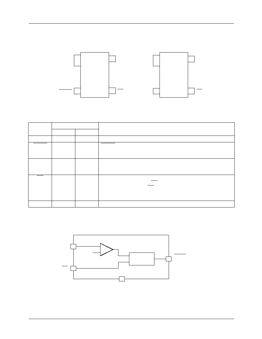
Typical Applications
FM811
FM812
µ
P
V
CC
V
CC
RESET
RESET
INPUT
MR
(RESET)
( ) = FM812
V
CC
FM811/812
Microprocessor Reset Circuits
FM811/812
2
REV. 1.5.1 7/15/02
Pr
eliminar
y Infor
mation
Pin Assignments
Pin Definitions
Internal Block Diagram
Pin Name
Pin Number
Description
FM811
FM812
GND
1
1
Ground Pin
RESET
2
N/A
RESET goes low if V
CC
falls below the reset threshold and remains
asserted for one reset time-out period (140ms min.) after V
CC
exceeds the
reset threshold.
RESET
N/A
2
RESET goes high if V
CC
falls below the reset threshold and remains
asserted for one reset time-out period (140ms min.) after V
CC
exceeds the
reset threshold.
MR
3
3
Manual reset input. Shorting this pin to GND forces a reset. The reset will
remain asserted as long as MR is held low and for one reset time-out
period (140ms min.) after MR goes high. This input cannot be driven by a
CMOS or TTL logic. Push-button switch is recommended to be used with
this pin. Float if unused.
V
CC
4
4
Power supply input, 3V, 3.3V, or 5V
FM811
V
CC
Top View
RESET
MR
2
4
3
FM812
V
CC
RESET
MR
GND
2
1
GND
1
4
3
4
3
Reset
Generator
2
1
≠
+
Reset
Threshold (V)
V
CC
MR
RESET (FM811)
RESET (FM812)
GND

FM811/812
REV. 1.5.1 7/15/02
3
Pr
eliminar
y Infor
mation
Absolute Maximum Ratings
Stresses above those listed under ABSOLUTE MAXIMUM RATINGS may cause permanent device failure. Functionality at or
above these limits is not implied. Exposure to absolute maximum ratings for extended periods may affect device reliability.
Operating ranges define those limits between which the functionality of the device is guaranteed.
Electrical Characteristics
V
CC
= 5V for FM81_L/M/J, V
CC
= 3.3V for FM81_S/T, V
CC
= 3V for FM81_R, T
A
= Operating Temperature Range,
unless otherwise noted.
Parameter
Symbol
Ratings
Units
Terminal Voltage
V
CC
-0.3 to 6.0
V
MR
-0.3 to (V
CC
+ 0.3)
V
Input Current
V
CC
, MR
20
mA
Output Current
RESET, RESET
20
mA
Rate of Rise
V
CC
100
V/µs
Operating Temperature Range
T
A
-40 to +85
∞C
Storage Temperature Range
-65 to +150
∞C
Lead Temperature Range
300
∞C
Power Dissipation (T
A
= +70∞C)
320
mW
Parameter
Conditions
Min.
Typ.
Max.
Units
Operating Voltage Range
T
A
= 0∞C to 70∞C
T
A
= -40∞C to 85∞C
1.4
1.6
5.5
5.5
V
Supply Current, I
CC
FM811L/M/J, FM812L/M/J
V
CC
< 3.6V, FM811R/S/T, FM812R/S/T
9
6
15
10
µA
Reset Voltage Threshold,
V
TH
FM811L, FM812L
FM811M, FM812M
FM811J, FM812J
FM811T, FM812T
FM811S, FM812S
FM811R, FM812R
4.40
4.18
3.90
2.97
2.79
2.49
4.63
4.38
4.00
3.08
2.93
2.63
4.86
4.52
4.18
3.19
3.00
2.70
V
Reset Time-out Period, t
R
140
240
560
ms
RESET Output Voltage, V
OH
I
SOURCE
= 800µA, FM811L/M/J
I
SOURCE
= 500µA, FM811R/S/T
V
CC
- 1.5
0.8 x V
CC
V
RESET Output Voltage, V
OL
V
CC
= V
TH
Min., I
SINK
= 3.2mA, FM811L/M/J
V
CC
= V
TH
Min., I
SINK
= 1.2mA, FM811R/S/T
V
CC
> 1.4V, I
SINK
= 50µA, T
A
= 0∞C to 70∞C
V
CC
> 1.6V, I
SINK
= 50µA, T
A
= -40∞C to
85∞C
0.4
0.3
0.3
0.3
V
RESET Output Voltage, V
OH
1.8V < V
CC
< V
TH
Min., I
SOURCE
= 150µA
0.8 x V
CC
V
RESET Output Voltage, V
OL
I
SINK
= 3.2mA, FM810L/M/J
I
SINK
= 1.2mA, FM810R/S/T
0.4
0.35
V
MR Minimum Pulse Width
10
µs
MR to Reset Delay
0.5
µs
MR Input Threshold, V
IH
V
CC
> V
TH
Max., FM81_L/M/J
FM81_R/S/T
2.3
0.7 x V
CC
V
MR Input Threshold, V
IL
V
CC
> V
TH
Max., FM81_L/M/J
FM81_R/S/T
0.8
0.25xV
CC
MR Pull-Up Resistance
10
20
30
k
MR Glitch Immunity
100
ns

FM811/812
4
REV. 1.5.1 7/15/02
Pr
eliminar
y Infor
mation
Circuit Description
Microprocessor Reset
The RESET pin is asserted whenever V
CC
falls below the
reset threshold voltage or if MR (manual reset) is forced low.
The reset pin remains asserted for a period of 40ms after
V
CC
has risen above the reset threshold voltage or MR has
returned high. The reset function ensures the microprocessor
is properly reset and powers up into a known condition after
a power failure. RESET will remain valid with V
CC
as low
as 1.4V.
V
CC
Transients
The FM811/ FM812 are relatively immune to negative-going
V
CC
glitches below the reset threshold. Typically, a negative-
going transient 125mV below the reset threshold with a
duration of 50ms (25ms for FM81_R/S/T) or less will not
cause an unwanted reset.
Manual Reset Function
Momentarily connecting the Manual Reset input pin (MR) to
GND forces a reset. Typically a Push-button switch is used
in most of the applications to force a manual reset. See
Typical Applications diagram. The reset will remain asserted
as long as MR is held low and for one reset time-out period
(140ms min.) after MR goes high. Note that this input cannot
be driven by a CMOS or TTL logic. This pin should be left
floating if manual reset feature is unused.
Interfacing to Bidirectional Reset Pins
The FM811/ FM812 can interface with µPs with
bidirectional reset pins by connecting a 4.7k
resistor in
series with the FM811/ FM812 output and the µP reset pin.
RESET Valid to 0V
A resistor can be added from the RESET pin to ground to
ensure the RESET output remains low with V
CC
down to 0V.
A 100k
resistor connected from RESET to ground is
recommended. The size of the resistor should be large
enough to not load the RESET output and small enough to
pull-down any stray leakage currents.
V
TH
V
CC
tR
MR
RESET
tR
FM811
µ
P
100k
V
CC
V
CC
RESET
RESET
V
CC
FM811/812
REV. 1.5.1 7/15/02
5
Pr
eliminar
y Infor
mation
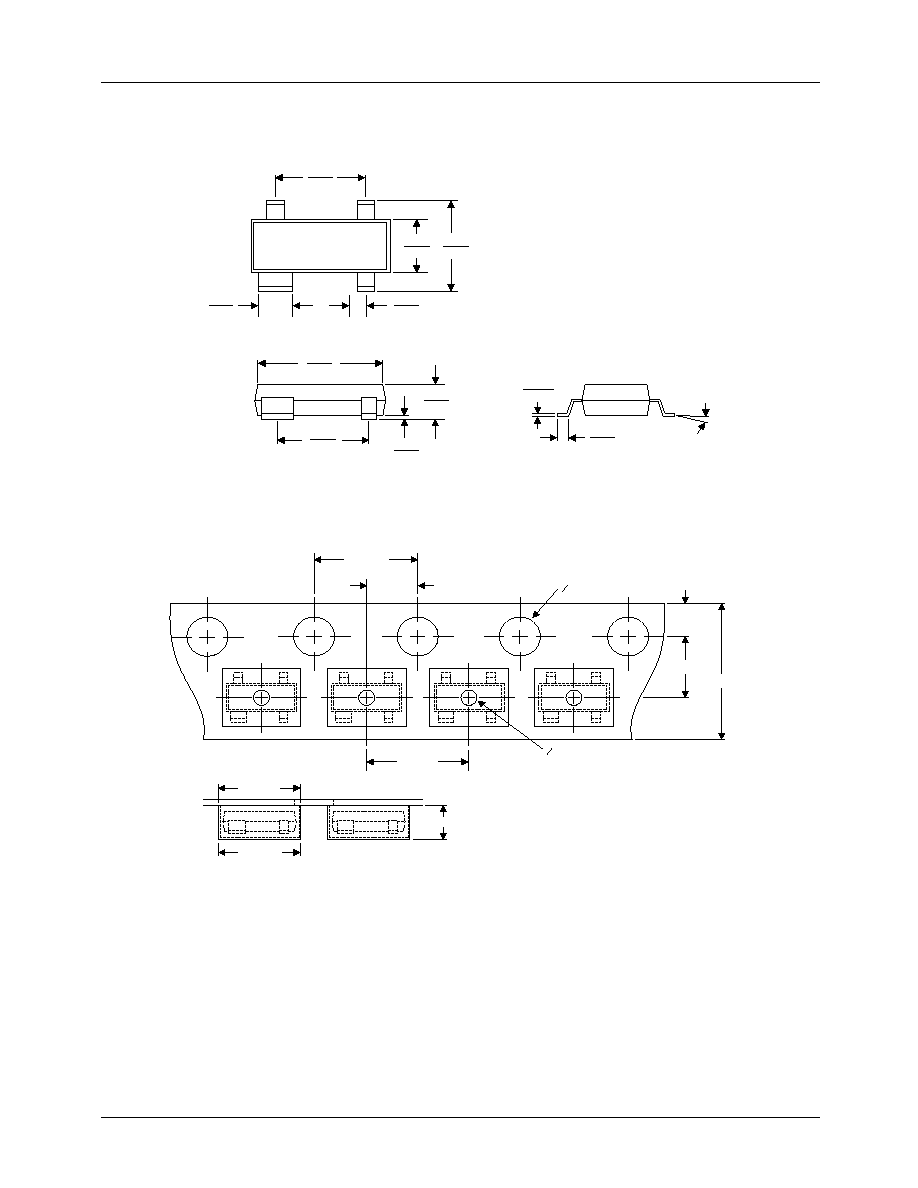
Packaging Information
4-Pin SOT-143
Tape and Reel Information
0.120
0.105
0.004
0.001
0.040
0.031
0.079
0.071
0.055
0.047
0.098
0.083
0.010
0.005
0.0059
0.0035
0.037
0.030
0.021
0.015
0.080
0.070
Dimensions are in inches
O1.5
±
0.1
3.5
±
0.05
8.0
±
0.3
1.75
±
0.1
4.0
±
0.1
2.0
±
0.05
4.0
±
0.1
O1.1
±
0.1
3.1
±
0.1
1.2
±
0.1
2.7
±
0.1
Dimensions are in millimeters