Äîêóìåíòàöèÿ è îïèñàíèÿ www.docs.chipfind.ru
©2005 Fairchild Semiconductor Corporation
www.fairchildsemi.com
Rev.1.0.0
Features
· Internal Avalanche Rugged Sense FET
· Low startup current (max 40uA)
· Low power consumption under 1 W at 240VAC & 0.4W
load
· Precise Fixed Operating Frequency (66kHz)
· Frequency Modulation for low EMI
· Pulse by Pulse Current Limiting (Adjustable)
· Over Voltage Protection (OVP)
· Over Load Protection (OLP)
· Thermal Shutdown Function (TSD)
· Auto-Restart Mode
· Under Voltage Lock Out (UVLO) with hysteresis
· Built-in Soft Start (15ms)
Application
· SMPS for VCR, SVR, STB, DVD & DVCD
· Adaptor
· SMPS for LCD Monitor
Description
The FSCM0565R is an integrated Pulse Width Modulator
(PWM) and Sense FET specifically designed for high
performance offline Switch Mode Power Supplies (SMPS)
with minimal external components. This device is an
integrated high voltage power switching regulator which
combine an avalanche rugged Sense FET with a current
mode PWM control block. The PWM controller includes
integrated fixed frequency oscillator, under voltage lockout,
leading edge blanking (LEB), optimized gate driver, internal
soft start, temperature compensated precise current sources
for a loop compensation and self protection circuitry.
Compared with discrete MOSFET and PWM controller
solution, it can reduce total cost, component count, size and
weight simultaneously increasing efficiency, productivity, and
system reliability. This device is a basic platform well suited
for cost effective designs of flyback converters.
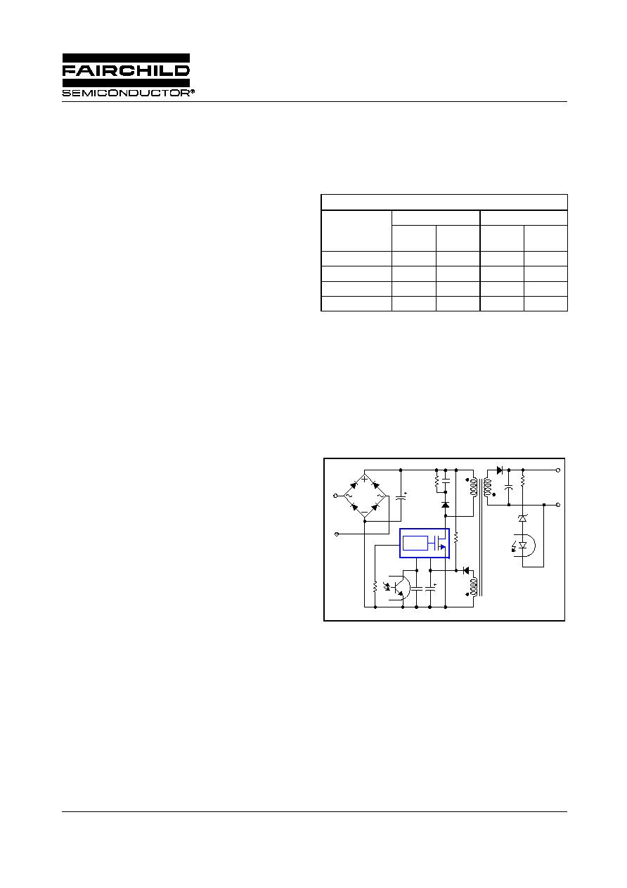
Table 1. Maximum Output Power
Notes:
1. Typical continuous power in a non-ventilated enclosed
adapter measured at 50
°
C ambient.
2. Maximum practical continuous power in an open frame
design at 50
°
C ambient.
3. 230 VAC or 100/115 VAC with doubler.
Typical Circuit
Figure 1. Typical Flyback Application
OUTPUT POWER TABLE
PRODUCT
230VAC
±
15%
(3)
85-265VAC
Adapt-
er
(1)
Open
Frame
(2)
Adapt-
er
(1)
Open
Frame
(2)
FSCM0565RD
50W
65W
40W
50W
FSCM0765RD
65W
70W
50W
60W
FSCM0565RC
70W
85W
60W
70W
FSCM0765RC
85W
95W
70W
85W
Drain
GND
Vfb
Vcc
PWM
AC
IN
DC
OUT
I
limit
FSCM0565R
Green Mode Fairchild Power Switch (FPS
TM
)
FSCM0565R
2
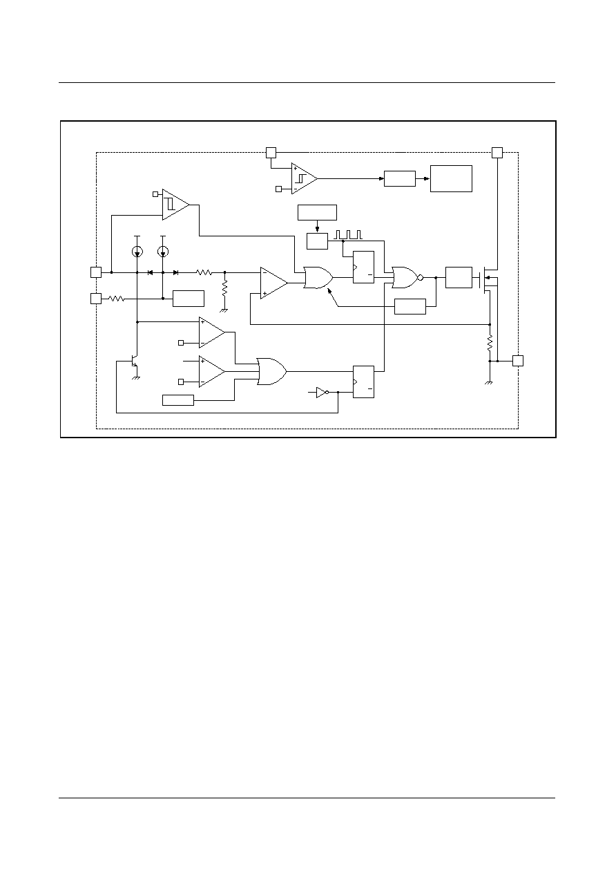
Internal Block Diagram
Figure 2. Functional Block Diagram of FSCM0565R
8V/12V
3
1
2
4
Vref
Internal
Bias
S
Q
Q
R
OSC
Vcc
Vcc
I
delay
I
FB
V
SD
TSD
Vovp
Vcc
S
Q
Q
R
R
2.5R
Vcc good
Vcc
Drain
FB
GND
Gate
driver
Vcc good
0.3/0.5V
LEB
PWM
Soft start
+
-
5
I
limit
Freq.
Modulation
Vcc UV reset
0.3K
FSCM0565R
3
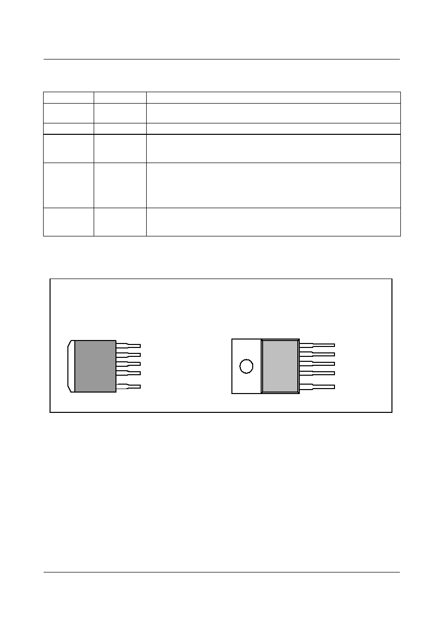
Pin Definitions
Pin Configuration
Figure 3. Pin Configuration (Top View)
Pin Number
Pin Name
Pin Function Description
1
Drain
This pin is the high voltage power SenseFET drain. It is designed to drive the
transformer directly.
2
GND
This pin is the control ground and the SenseFET source.
3
Vcc
This pin is the positive supply voltage input. Initially, During start up, the power is
supplied through the startup resistor from DC link. When Vcc reaches 12V, the
power is supplied from auxiliary transformer winding.
4
Feedback (FB)
This pin is internally connected to the inverting input of the PWM comparator.
The collector of an optocoupler is typically tied to this pin. For stable operation, a
capacitor should be placed between this pin and GND. If the voltage of this pin
reaches 6.0V, the over load protection is activated resulting in shutdown of the
FPS.
5
I_limit
This pin is for the pulse by pulse current limit level programming. By using a
resistor to GND on this pin, the current limit level can be changed. If this pin is
left floating, the typical current limit will be 2.5A.
FSC
M
056
5R
D
1 : Drain
2 : GND
5 : I_limit
4 : FB
3 : Vcc
D2-PAK-5L
F
S
C
M
0565R
C
F
S
C
M
0565R
C
F
S
C
M
0565R
C
F
S
C
M
0565R
C
1. Drain
2. GND
3. Vcc
4. FB
5. I_limit
TO-220-5L
FSCM0565RD
FSCM0565RC

FSCM0565R
4
Absolute Maximum Ratings
(Ta=25
°
C, unless otherwise specified)
Notes:
1. T
j
= 25
°
C to 150
°
C
2. Repetitive rating: Pulse width limited by maximum junction temperature
3. L = 30mH, V
DD
= 50V, R
G
= 25
, starting T
j
= 25
°
C
4. L = 13uH, starting T
j
= 25
°
C
Parameter
Symbol
Value
Unit
Drain-Source (GND) Voltage
(1)
V
DSS
650
V
Drain-Gate Voltage (R
GS
=1M
)
V
DGR
650
V
Gate-Source (GND) Voltage
V
GS
±
30
V
Drain Current Pulsed
(2)
I
DM
20
A
DC
Continuous Drain Current (TO-220)
@ Tc = 25°C
@ T
C
=100
°
C
I
D
5
A
DC
I
D
3.2
A
DC
Continuous Drain Current (D2-PAK)
@ Tc = 25°C
@ T
C
=100
°
C
I
D
2.9
A
DC
I
D
1.9
A
DC
Supply Voltage
V
CC
20
V
Analog Input Voltage Range
V
FB
-0.3 to V
CC
V
Total Power Dissipation (D2-PAK)
P
D
75
W
Derating
0.6
W/
°
C
Total Power Dissipation (TO-220)
P
D
120
W
Derating
0.96
W/
°
C
Operating Junction Temperature
T
J
Internally limited
°
C
Operating Ambient Temperature
T
A
-25 to +85
°
C
Storage Temperature Range
T
STG
-55 to +150
°
C
ESD Capability, HBM Model (All pins
excepts for Vstr and Vfb)
-
2.0
(Vcc-Vfb=1.0kV)
kV
ESD Capability, Machine Model (All pins
excepts for Vstr and Vfb)
-
300
(Vcc-Vfb=100V)
V

FSCM0565R
5
Electrical Characteristics
(Ta = 25
°
C unless otherwise specified)
Parameter Symbol
Condition
Min.
Typ.
Max.
Unit
Sense FET SECTION
Drain source breakdown voltage
BV
DSS
V
GS
= 0V, I
D
= 250
µ
A
650
-
-
V
Zero gate voltage drain current
I
DSS
V
DS
= Max, Rating
V
GS
= 0V
-
-
500
µ
A
Static drain source on resistance
R
DS(ON)
V
GS
= 10V, I
D
= 2.3A
-
1.76
2.2
Output capacitance
C
OSS
V
GS
= 0V, V
DS
= 25V,
f = 1MHz
-
78
-
pF
Turn on delay time
T
D(ON)
V
DD
= 325V, I
D
= 5A
(MOSFET switching
time is essentially
independent of
operating temperature)
-
22
-
ns
Rise time
T
R
-
52
-
Turn off delay time
T
D(OFF)
-
95
-
Fall time
T
F
-
50
-
CONTROL SECTION
Initial frequency
F
OSC
V
CC
=14V, V
FB
=5V
60
66
72
kHz
Modulated frequency range
F
mod
-
-
±3
-
kHz
Frequency modulation cycle
T
mod
-
-
4
-
ms
Voltage stability
F
STABLE
10V
V
CC
17V
0
1
3
%
Temperature stability
F
OSC
-
25
°
C
Ta
+85
°
C
-
±5
±10
%
Maximum duty cycle
D
MAX
-
75
80
85
%
Minimum duty cycle
D
MIN
-
-
-
0
%
Start threshold voltage
V
START
V
FB
=GND
11
12
13
V
Stop threshold voltage
V
STOP
V
FB
=GND
7
8
9
V
Feedback source current
I
FB
V
FB
=GND
0.7
0.9
1.1
mA
Soft-start time
T
SS
-
10
15
20
ms
BURST MODE SECTION
Burst Mode Voltages
V
BH
Vcc=14V
0.4
0.5
0.6
V
VB
L
Vcc=14V
0.24
0.3
0.36
V

FSCM0565R
6
Notes:
1. Pulse test : Pulse width
300
µ
S, duty
2%
2. These parameters, although guaranteed at the design, are not tested in mass production.
3. These parameters, although guaranteed, are tested in EDS (wafer test) process.
4. These parameters indicate the inductor current.
5. This parameter is the current flowing into the control IC.
PROTECTION SECTION
Peak current limit
I
LIM
V
CC
=14V, V
FB
=5V
2.2
2.5
2.8
A
Over voltage protection
V
OVP
-
18
19
20
V
Thermal shutdown temperature
T
SD
130
145
160
°
C
Shutdown delay current
I
DELAY
V
FB
=4V
3.5
5.3
7
µ
A
Shutdown feedback voltage
V
SD
V
FB
>5.5V
5.5
6
6.5
V
TOTAL DEVICE SECTION
Startup current
I
start
-
20
40
µ
A
Operating supply current
I
OP(MIN)
V
CC
=10V, V
FB
=0V
-
2.5
5
mA
I
OP(MAX)
V
CC
=20V, V
FB
=0V

FSCM0565R
7
Comparison Between FSDM0565RB and FSCM0565R
Function
FSDM0565RB
FSCM0565R
Frequency modulation
N.A.
Available
· Modulated frequency range (DF
mod
) = ±3kHz
· Frequency modulation cycle (T
mod
) = 4ms
Pulse-by-pulse current limit · Internally fixed (2.25A)
· Programmable using external resistor (2.5A max)
Internal Startup Circuit
· Available
· N.A. (Requires startup resistor)
· Startup current : 40uA (max)
FSCM0565R
8
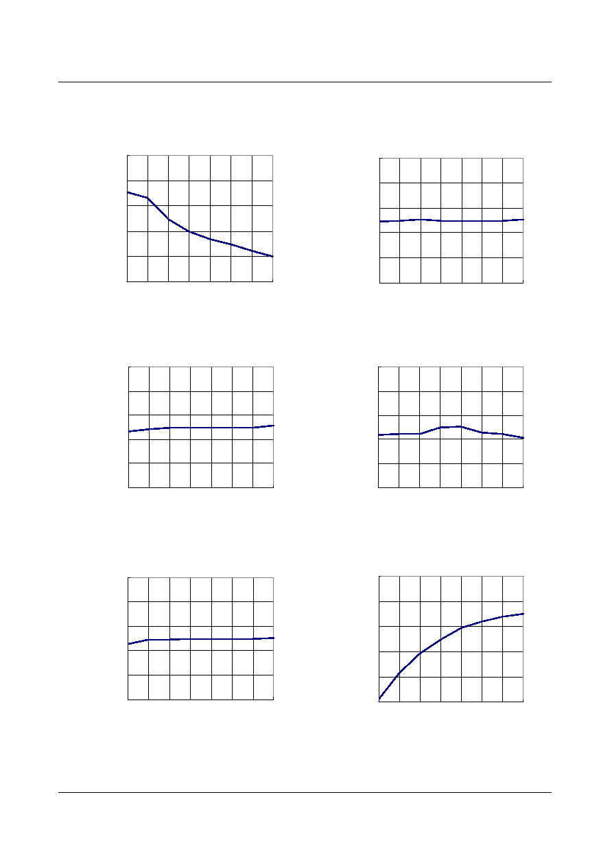
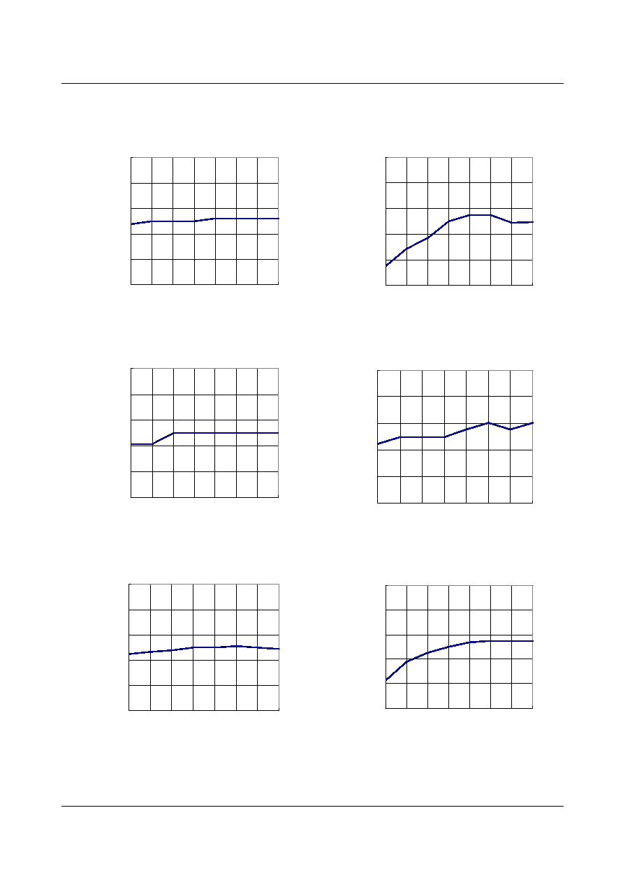
Typical Performance Characteristics
(These Characteristic Graphs are Normalized at Ta= 25
°
C)
Startup Current vs. Temp
Start Threshold Voltage vs. Temp
Stop Threshold Voltage vs. Temp
Initial Freqency vs. Temp
Maximum Duty Cycle vs. Temp
Feedback Source Current vs. Temp
0.60
0.80
1.00
1.20
1.40
1.60
-50
-25
0
25
50
75
100 125
Junction Temperature()
S
t
a
r
t
up C
u
r
r
e
n
t
(
N
o
r
m
a
l
i
zed
t
o
2
5
)
0.80
0.88
0.96
1.04
1.12
1.20
-50
-25
0
25
50
75
100 125
Junction T emperature()
S
t
a
r
t
T
h
r
e
s
hol
d
V
o
l
t
a
ge
(
N
or
ma
l
i
z
e
d
t
o
25
)
0.80
0.88
0.96
1.04
1.12
1.20
-50
-25
0
25
50
75
100 125
Junction Temperature()
S
t
op T
h
r
e
s
hol
d V
o
l
t
a
g
e
(
N
o
r
m
a
liz
e
d
to
2
5
)
0.80
0.88
0.96
1.04
1.12
1.20
-50
-25
0
25
50
75
100 125
Junction Temperature()
I
n
itia
l F
r
e
q
u
e
n
c
y
(
N
o
r
m
a
lize
d
to
2
5
)
0.80
0.88
0.96
1.04
1.12
1.20
-50
-25
0
25
50
75
100 125
Junction Temperature()
M
a
xi
mu
m D
u
t
y
C
y
c
l
e
(
N
o
r
m
a
lize
d
to
2
5
)
0.80
0.88
0.96
1.04
1.12
1.20
-50
-25
0
25
50
75
100
125
Junction T emperature()
F
B
S
o
u
r
ce C
u
r
r
en
t
(
N
o
r
m
a
liz
e
d
to
2
5
)
FSCM0565R
9
Typical Performance Characteristics
(Continued)
(These Characteristic Graphs are Normalized at Ta= 25
°
C)
ShutDown Feedback Voltage vs. Temp
ShutDown Delay Current vs. Temp
Bust Mode Enable Volage vs. Temp
Burst Mode Disable Voltage vs. Temp
Mavimum Drain Current vs. Temp
Operating Supply Current vs. Temp
0.80
0.88
0.96
1.04
1.12
1.20
-50
-25
0
25
50
75
100
125
Junction Temperature()
S
h
ut
d
o
w
n F
B
V
o
l
t
a
g
e
(
N
o
r
m
a
liz
e
d
to
2
5
)
0.80
0.88
0.96
1.04
1.12
1.20
-50
-25
0
25
50
75
100
125
Junction T emperature()
S
h
ut
do
w
n
D
e
l
a
y
C
u
r
r
e
n
t
(
N
o
r
m
a
liz
e
d
to
2
5
)
0.80
0.88
0.96
1.04
1.12
1.20
-50
-25
0
25
50
75
100
125
Junction T emperature()
B
u
r
s
t
M
o
d
e
E
n
a
b
le
V
o
lt
a
g
e
(
N
o
r
m
a
li
zed
to
2
5
)
0.80
0.88
0.96
1.04
1.12
1.20
-50
-25
0
25
50
75
100
125
Junction Temperature()
B
u
r
s
t
M
ode
D
i
s
a
bl
e
V
o
l
t
a
g
e
(
N
o
r
m
a
lize
d
to
2
5
)
0.80
0.88
0.96
1.04
1.12
1.20
-50
-25
0
25
50
75
100
125
Junction Temperature()
M
a
xi
mum D
r
a
i
n C
u
r
r
e
n
t
(
N
o
r
m
a
liz
e
d
to
2
5
)
0.80
0.88
0.96
1.04
1.12
1.20
-50
-25
0
25
50
75
100 125
Junction Temperature()
O
p
e
r
a
t
i
n
g S
upp
l
y
C
u
r
r
e
nt
(
N
or
m
a
l
i
z
e
d
t
o
25
)
FSCM0565R
10
Functional Description
1.
1.
1.
1.
Startup : Figure 4 shows the typical startup circuit and
transformer auxiliary winding for FSCM0565R application.
Before FSCM0565R begins switching, FSCM0565R
consumes only startup current (typically 25uA) and the
current supplied from the DC link supply ccurrent consumed
by FPS (Icc) and charges the external capacitor (C
a
) that is
connected to the Vcc pin. When Vcc reaches start voltage of
12V (V
START
), FSCM0565R begins switching, and the
current consumed by FSCM0565R increases to 3mA. Then,
FSCM0565R continues its normal switching operation and
the power required for this device is supplied from the
transformer auxiliary winding, unless Vcc drops below the
stop voltage of 8V (V
STOP
). To guarantee the stable operation
of the control IC, Vcc has under voltage lockout (UVLO)
with 4V hysteresis. Figure 5 shows the relation between the
current consumed by FPS (Icc) and the supply voltage (Vcc).
Figure 4. Startup circuit
Figure 5. Relation between operating supply current and
Vcc voltage
The minimum current supplied through the startup resistor is
given by
where V
line
min
is the minimum input voltage, V
start
is the
start voltage (12V) and R
str
is the startup resistor. The startup
resistor should be chosen so that I
sup
min
is larger than the
maximum startup current (40uA). If not, Vcc can not be
charged to the start voltage and FPS will fail to start up.
2. Feedback Control : FSCM0565R employs current mode
control, as shown in Figure 6. An opto-coupler (such as the
H11A817A) and shunt regulator (such as the KA431) are
typically used to implement the feedback network.
Comparing the feedback voltage with the voltage across the
Rsense resistor makes it possible to control the switching
duty cycle. When the reference pin voltage of the KA431
exceeds the internal reference voltage of 2.5V, the
H11A817A LED current increases, thus pulling down the
feedback voltage and reducing the duty cycle. This event
typically happens when the input voltage is increased or the
output load is decreased.
2.1 Pulse-by-pulse current limit: Because current mode
control is employed, the peak current through the Sense FET
is determined by the inverting input of PWM comparator
(Vfb*) as shown in Figure 6. When the current through the
opto transistor is zero and the current limit pin (#5) is left
floating, the feedback current source (I
FB
) of 0.9mA flows
only through the internal resistor (R+2.5R=2.8k). In this
case, the cathode voltage of diode D2 and the peak drain
current have maximum values of 2.5V and 2.5A, respec-
tively. The pulse-by-pulse current limit can be adjusted using
a resistor to GND on current limit pin (#5). The current limit
level using an external resistor (R
LIM
) is given by
Figure 6. Pulse width modulation (PWM) circuit
FSCM0565R
Rstr
Vcc
Ca
Da
I
sup
AC line
(V
line
min
- V
line
max
)
C
DC
I
cc
Icc
Vcc
Vstop=8V
25uA
3mA
Vstart=12V
Vz
Power Up
Power Down
Isup
min
2 V
line
min
V
start
(
)
1
Rstr
------------
=
I
LIM
R
LIM
2.5A
2.8k
R
LIM
+
------------------------------------
=
4
OSC
Vcc
Vref
I
delay
I
FB
V
SD
R
2.5R
Gate
driver
OLP
D1
D2
+
V
fb
*
-
Vfb
KA431
C
B
Vo
H11A817A
R
sense
SenseFET
5
R
LI M
0.9mA
0.3k
FSCM0565R
11
2.2 Leading edge blanking (LEB) : At the instant the
internal Sense FET is turned on, there usually exists a high
current spike through the Sense FET, caused by primary-side
capacitance and secondary-side rectifier reverse recovery.
Excessive voltage across the Rsense resistor would lead to
incorrect feedback operation in the current mode PWM
control. To counter this effect, the FSCM0565R employs a
leading edge blanking (LEB) circuit. This circuit inhibits the
PWM comparator for a short time (T
LEB
) after the Sense FET
is turned on.
3. Protection Circuit : The FSCM0565R has several self
protective functions such as over load protection (OLP), over
voltage protection (OVP) and thermal shutdown (TSD).
Because these protection circuits are fully integrated into the
IC without external components, the reliability can be
improved without increasing cost. Once the fault condition
occurs, switching is terminated and the Sense FET remains
off. This causes Vcc to fall. When Vcc reaches the UVLO
stop voltage of 8V, the current consumed by FSCM0565R
reduces to the startup current (typically 25uA) and the
current supplied from the DC link charges the external
capacitor (C
a
) that is connected to the Vcc pin. When Vcc
reaches the start voltage of 12V, FSCM0565R resumes its
normal operation. In this manner, the auto-restart can
alternately enable and disable the switching of the power
Sense FET until the fault condition is eliminated (see Figure
7).
Figure 7. Auto restart operation
3.1 Over Load Protection (OLP) : Overload is defined as
the load current exceeding a pre-set level due to an
unexpected event. In this situation, the protection circuit
should be activated in order to protect the SMPS. However,
even when the SMPS is in the normal operation, the over
load protection circuit can be activated during the load
transition. In order to avoid this undesired operation, the over
load protection circuit is designed to be activated after a
specified time to determine whether it is a transient situation
or an overload situation. Because of the pulse-by-pulse
current limit capability, the maximum peak current through
the Sense FET is limited, and therefore the maximum input
power is restricted with a given input voltage. If the output
consumes beyond this maximum power, the output voltage
(Vo) decreases below the set voltage. This reduces the
current through the opto-coupler LED, which also reduces
the opto-coupler transistor current, thus increasing the
feedback voltage (Vfb). If Vfb exceeds 2.5V, D1 is blocked
and the 5.3uA current source (I
delay
) starts to charge C
B
slowly up to Vcc. In this condition, Vfb continues increasing
until it reaches 6V, when the switching operation is
terminated as shown in Figure 8. The delay time for
shutdown is the time required to charge C
B
from 2.5V to
6.0V with 5.3uA (I
delay
). In general, a 10 ~ 50 ms delay time
is typical for most applications.
Figure 8. Over load protection
3.2 Over voltage Protection (OVP) : If the secondary side
feedback circuit were to malfunction or a solder defect
caused an open in the feedback path, the current through the
opto-coupler transistor becomes almost zero. Then, Vfb
climbs up in a similar manner to the over load situation,
forcing the preset maximum current to be supplied to the
SMPS until the over load protection is activated. Because
more energy than required is provided to the output, the
output voltage may exceed the rated voltage before the over
load protection is activated, resulting in the breakdown of the
devices in the secondary side. In order to prevent this
situation, an over voltage protection (OVP) circuit is
employed. In general, Vcc is proportional to the output
voltage and the FSCM0565R uses Vcc instead of directly
monitoring the output voltage. If V
CC
exceeds 19V, an OVP
circuit is activated resulting in the termination of the
switching operation. In order to avoid undesired activation of
OVP during normal operation, Vcc should be designed to be
below 19V.
Fault
situation
8V
12V
Vcc
Vds
t
Fault
occurs
Fault
removed
Normal
operation
Normal
operation
Power
on
V
V
V
V
FB
FB
FB
FB
t
t
t
t
2.5V
2.5V
2.5V
2.5V
6.0V
6.0V
6.0V
6.0V
Over load protection
Over load protection
Over load protection
Over load protection
T
T
T
T
12
12
12
12
= Cfb*(6.0-2.5)/I
= Cfb*(6.0-2.5)/I
= Cfb*(6.0-2.5)/I
= Cfb*(6.0-2.5)/I
delay
delay
delay
delay
T
T
T
T
1
1
1
1
T
T
T
T
2
2
2
2
FSCM0565R
12
3.3 Thermal Shutdown (TSD) : The Sense FET and the
control IC are built in one package. This makes it easy for
the control IC to detect the heat generation from the Sense
FET. When the temperature exceeds approximately 145
°
C,
the thermal protection is triggered resulting in shutdown of
FPS.
4. Frequency Modulation : EMI reduction can be
accomplished by modulating the switching frequency of a
switched power supply. Frequency modulation can reduce
EMI by spreading the energy over a wider frequency range
than the band width measured by the EMI test equipment.
The amount of EMI reduction is directly related to the depth
of the reference frequency. As can be seen in Figure 9, the
frequency changes from 63KHz to 69KHz in 4ms.
Figure 9. Frequency Modulation
5. Soft Start : The FSCM0565R has an internal soft start
circuit that increases PWM comparator inverting input
voltage together with the Sense FET current slowly after it
starts up. The typical soft start time is 15msec, The pulse
width to the power switching device is progressively
increased to establish the correct working conditions for
transformers, rectifier diodes and capacitors. The voltage on
the output capacitors is progressively increased with the
intention of smoothly establishing the required output
voltage. It also helps to prevent transformer saturation and
reduce the stress on the secondary diode during startup.
6. Burst operation : In order to minimize power dissipation
in standby mode, the FSCM0565R enters into burst mode
operation at light load condition. As the load decreases, the
feedback voltage decreases. As shown in Figure 10, the
device automatically enters into burst mode when the
feedback voltage drops below V
BL
(300mV). At this point
switching stops and the output voltages start to drop at a rate
dependent on standby current load. This causes the feedback
voltage to rise. Once it passes V
BH
(500mV) switching
resumes. The feedback voltage then falls and the process
repeats. Burst mode operation alternately enables and
disables switching of the power Sense FET thereby reducing
switching loss in standby mode.
Figure 10. Waveforms of burst operation
T
s
T
s
T
s
Drain current
f
s
66kHz
69kHz
63kHz
4ms
t
V
FB
Vds
0.3V
0.5V
Ids
Vo
Vo
set
time
Switching
disabled
T1
T2 T3
Switching
disabled
T4
FSCM0565R
13
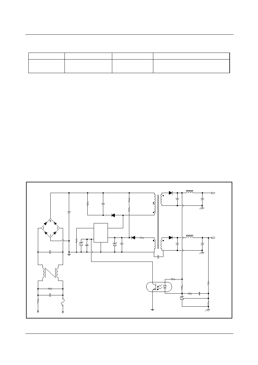
Typical application circuit
Features
· High efficiency (>81% at 85Vac input)
· Low standby mode power consumption (<1W at 240Vac input and 0.4W load)
· Low component count
· Enhanced system reliability through various protection functions
· Low EMI through frequency modulation
· Internal soft-start (15ms)
Key Design Notes
· The delay time for over load protection is designed to be about 50ms with C106 of 47nF. If a faster triggering of OLP is
required, C106 can be reduced to 22nF.
· Using a resistor R106 on the current limit pin (#5), the pule-by-pulse current limit level is reduced to about 2A.
· Zener diode ZD102 is used for a safety test such as UL. When the drain pin and feedback pin are shorted, the zener diode
fails and remains short, which causes the fuse (F1) blown and prevents explosion of the opto-coupler (IC301). This zener
diode also increases the immunity against line surge.
1. Schematic
Application
Output power
Input voltage
Output voltage (Max current)
LCD Monitor
40W
Universal input
(85-265Vac)
5V (2.0A)
12V (2.5A)
3
4
C102
220nF
275VAC
LF101
23mH
C101
220nF
275VAC
RT1
5D-9
F1
FUSE
250V
2A
C103
100uF
400V
R103
56k
2W
C104
2.2nF
1kV
D101
UF 4007
C106
47nF
50V
C105
22uF
50V
D102
TVR10G
R104
5
1
2
3
4
5
T1
EER3016
BD101
2KBP06M3N257
1
2
R101
560k
1W
FSCM0565RC
I
limit
Vfb
Vcc
Drain
GND
1
2
3
4
5
ZD101
22V
8
10
D202
MBRF10100
C201
1000uF
25V
C202
1000uF
25V
L201
12V, 2.5A
6
7
D201
MBRF1045
C203
1000uF
10V
C204
1000uF
10V
L202
5V, 2A
R201
1k
R202
1.2k
R204
5.6k
R203
10k
C205
47nF
R205
5.6k
C301
4.7nF
IC301
H11A817A
IC201
KA431
R102
500k
R105
500k
R106
10k
1/4W
ZD102
10V
FSCM0565R
14
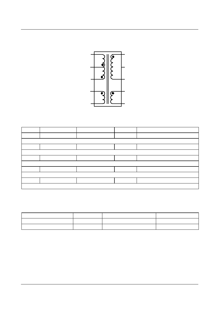
2. Transformer Schematic Diagram
3.Winding Specification
4.Electrical Characteristics
5. Core & Bobbin
Core : EER 3016
Bobbin : EER3016
Ae(mm2) : 96
No
Pin (s
f)
Wire
Turns
Winding Method
Na
4
5
0.2
×
1
8
Center Winding
Insulation: Polyester Tape t = 0.050mm, 2Layers
Np/2
2
1
0.4
×
1
18
Solenoid Winding
Insulation: Polyester Tape t = 0.050mm, 2Layers
N
12V
10
8
0.3
×
3
7
Center Winding
Insulation: Polyester Tape t = 0.050mm, 2Layers
N5V
7
6
0.3
×
3
3
Center Winding
Insulation: Polyester Tape t = 0.050mm, 2Layers
Np/2
3
2
0.4
×
1
18
Solenoid Winding
Outer Insulation: Polyester Tape t = 0.050mm, 2Layers
Pin
Specification
Remarks
Inductance
1 - 3
570uH ± 10%
100kHz, 1V
Leakage Inductance
1 - 3
10uH Max
2
nd
all short
EER3016
N
p
/2
N
12V
N
a
1
2
3
4
5
6
7
8
9
10
N
p
/2
N
5V

FSCM0565R
15
6.Demo Circuit Part List
Part
Value
Note
Part
Value
Note
Fuse
C301
4.7nF
Polyester Film Cap.
F101
2A/250V
NTC
Inductor
RT101
5D-9
L201
5uH
Wire 1.2mm
Resistor
L202
5uH
Wire 1.2mm
R101
560K
1W
R102
500K
1/4W
R103
56K
2W
R104
5
1/4W
Diode
R105
500K
1/4W
D101
UF4007
R106
10K
1/4W
D102
TVR10G
R201
1K
1/4W
D201
MBRF1045
R202
10K
1/4W
D202
MBRF10100
R203
1.2K
1/4W
ZD101
22V Zener diode
R204
5.6K
1/4W
ZD102
10V Zener diode
R205
5.6K
1/4W
Bridge Diode
BD101
2KBP06M 3N257
Bridge Diode
Capacitor
C101
220nF/275VAC
Box Capacitor
Line Filter
C102
220nF/275VAC
Box Capacitor
LF101
23mH
Wire 0.4mm
C103
100uF/400V
Electrolytic Capacitor
IC
C104
10nF/1kV Ceramic
Capacitor
IC101
FSCM0565RC
FPS
TM
(7A,650V)
C105
22uF/50V
Electrolytic Capacitor
IC201
KA431(TL431)
Voltage reference
C106
47nF/50V
Ceramic Capacitor
IC301
H11A817A
Opto-coupler
C201
1000uF/25V
Electrolytic Capacitor
C202
1000uF/25V
Electrolytic Capacitor
C203
1000uF/10V
Electrolytic Capacitor
C204
1000uF/10V
Electrolytic Capacitor
C205
47nF/50V
Ceramic Capacitor
FSCM0565R
16
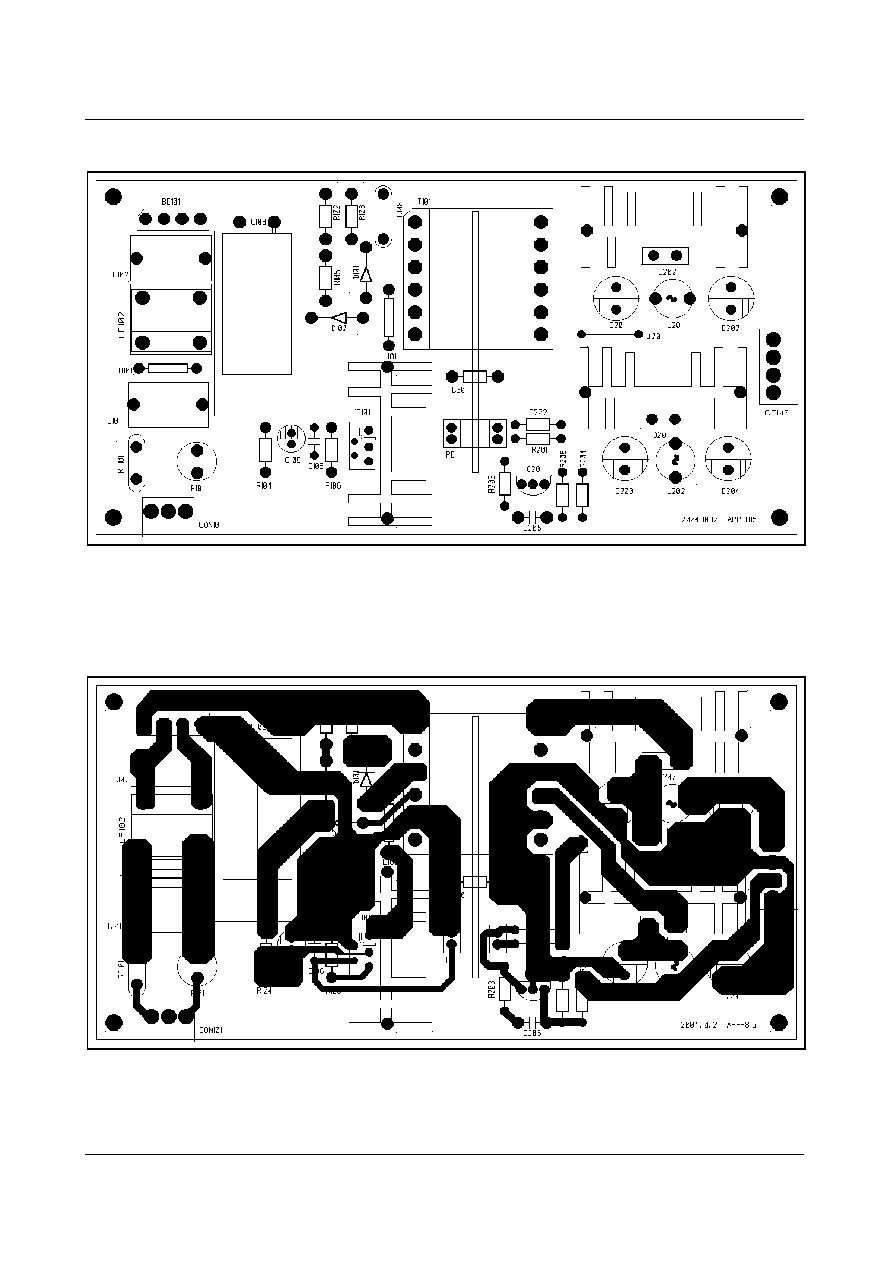
7. Layout
Figure 11. Layout Considerations for FSCM0565RC
Figure 12. Layout Considerations for FSCM0565RC
FSCM0565R
17
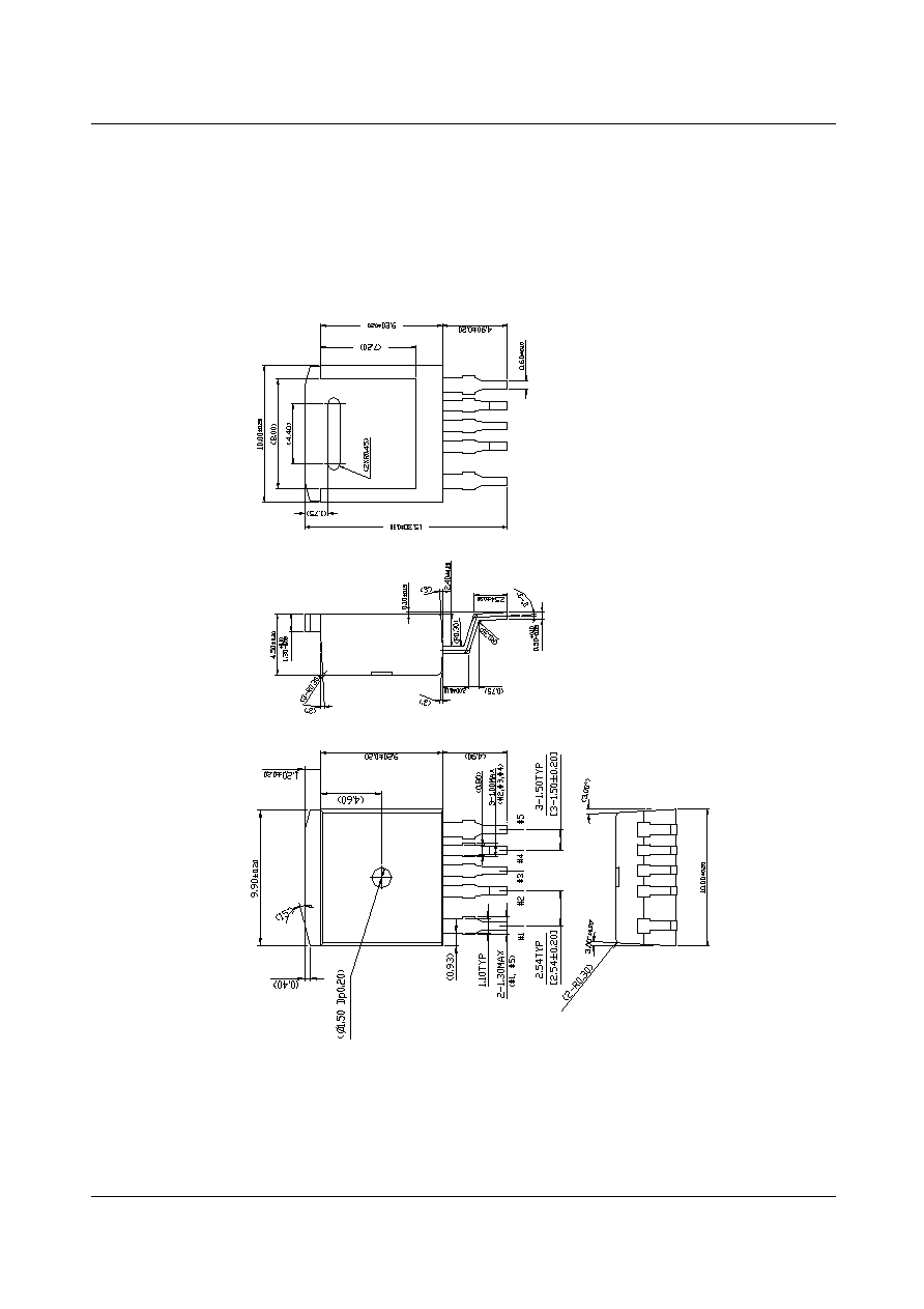
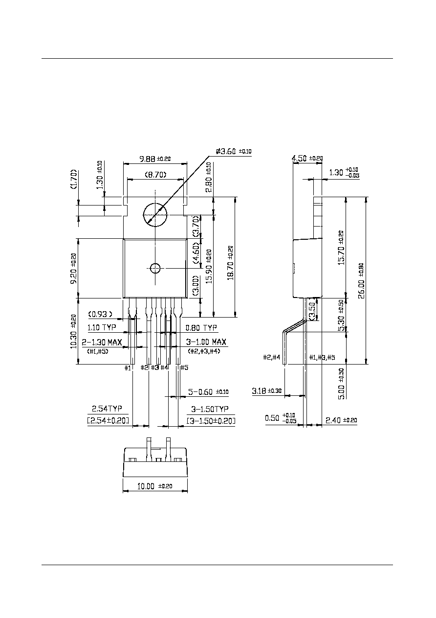
Package Dimensions
D2-PAK-5L
FSCM0565R
18
Package Dimensions
(Continued)
TO-220-5L(Forming)

FSCM0565R
19
Ordering Information
Product Number
Package
Marking Code
BVdss
Rds(on)Max.
FSCM0565RD
D2-PAK-5L
CM0565RD
650V
2.2
FSCM0565RCYDTU
TO-220-5L
CM0565RC
650V
2.2

FSCM0565R
1/13/05 0.0m 001
2005 Fairchild Semiconductor Corporation
LIFE SUPPORT POLICY
FAIRCHILD'S PRODUCTS ARE NOT AUTHORIZED FOR USE AS CRITICAL COMPONENTS IN LIFE SUPPORT DEVICES
OR SYSTEMS WITHOUT THE EXPRESS WRITTEN APPROVAL OF THE PRESIDENT OF FAIRCHILD SEMICONDUCTOR
CORPORATION. As used herein:
1. Life support devices or systems are devices or systems
which, (a) are intended for surgical implant into the body,
or (b) support or sustain life, and (c) whose failure to
perform when properly used in accordance with
instructions for use provided in the labeling, can be
reasonably expected to result in a significant injury of the
user.
2. A critical component in any component of a life support
device or system whose failure to perform can be
reasonably expected to cause the failure of the life support
device or system, or to affect its safety or effectiveness.
www.fairchildsemi.com
DISCLAIMER
FAIRCHILD SEMICONDUCTOR RESERVES THE RIGHT TO MAKE CHANGES WITHOUT FURTHER NOTICE TO ANY
PRODUCTS HEREIN TO IMPROVE RELIABILITY, FUNCTION OR DESIGN. FAIRCHILD DOES NOT ASSUME ANY
LIABILITY ARISING OUT OF THE APPLICATION OR USE OF ANY PRODUCT OR CIRCUIT DESCRIBED HEREIN; NEITHER
DOES IT CONVEY ANY LICENSE UNDER ITS PATENT RIGHTS, NOR THE RIGHTS OF OTHERS.