Äîêóìåíòàöèÿ è îïèñàíèÿ www.docs.chipfind.ru
©2005 Fairchild Semiconductor Corporation
www.fairchildsemi.com
Rev.1.1.0
Features
· Internal Avalanche Rugged SenseFET
· Low Start-up Current (max 40uA)
· Low Power Consumption under 1 W at 240VAC and
0.4W Load
· Precise Fixed Operating Frequency (66kHz)
· Frequency Modulation for low EMI
· Pulse by Pulse Current Limiting (Adjustable)
· Over Voltage Protection (OVP)
· Over Load Protection (OLP)
· Thermal Shutdown Function (TSD)
· Auto-Restart Mode
· Under Voltage Lock Out (UVLO) with Hysteresis
· Built-in Soft Start (15ms)
Application
· SMPS for VCR, SVR, STB, DVD and
DVCD
· Adaptor
· SMPS for LCD Monitor
Related Application Notes
·
AN-4137
: Design Guidelines for Off-line Flyback
Converters Using Fairchild Power Switch (FPS)
·
AN-4140
: Transformer Design Consideration for off-line
Flyback Converters using Fairchild Power Switch
·
AN-4141
: Troubleshooting and Design Tips for Fairchild
Power Switch Flyback Applications
·
AN-4148
: Audible Noise Reduction Techniques for FPS
Applications
Description
The FSCM0765R is an integrated Pulse Width Modulator
(PWM) and SenseFET specifically designed for high
performance offline Switch Mode Power Supplies (SMPS)
with minimal external components. This device is an
integrated high voltage power switching regulator which
combines
an avalanche rugged SenseFET with a current
mode PWM control block. The PWM controller includes
integrated fixed frequency oscillator, under voltage lockout,
leading edge blanking (LEB), optimized gate driver, internal
soft start, temperature compensated precise current sources
for a loop compensation, and self protection circuitry.
Compared with a discrete MOSFET and PWM controller
solution, it can reduce total cost, component count, size
,
and
weight while simultaneously increasing efficiency, productivity,
and system reliability. This device is a basic platform well
suited for cost effective designs of flyback converters.
Table 1. Maximum Output Power
Notes:
1. Typical continuous power in a non-ventilated enclosed
adapter measured at 50
°
C ambient.
2. Maximum practical continuous power in an open-frame
design at 50
°
C ambient.
3. 230 VAC or 100/115 VAC with doubler.
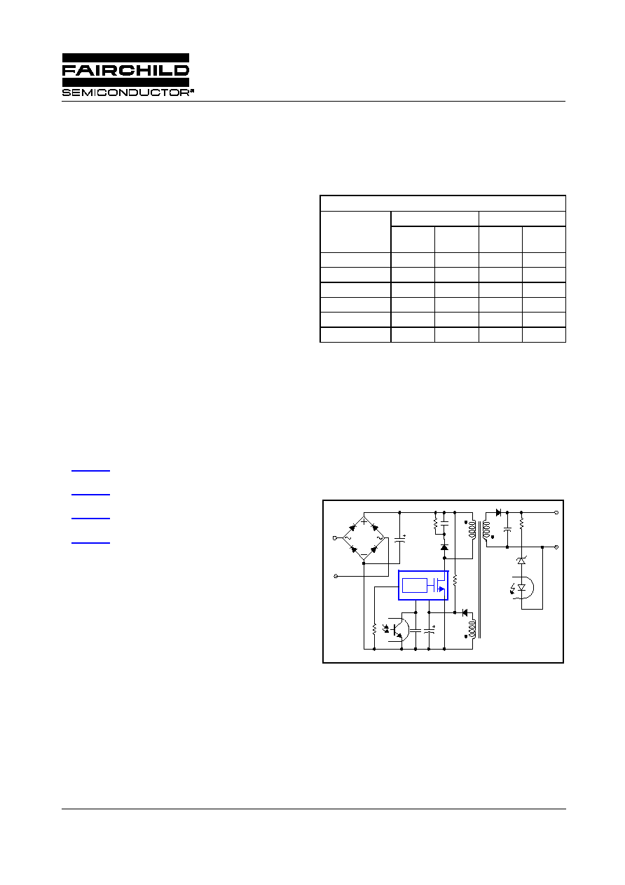
Typical Circuit
Figure 1. Typical Flyback Application
OUTPUT POWER TABLE
PRODUCT
230VAC
±
15%
(3)
85-265VAC
Adapt-
er
(1)
Open
Frame
(2)
Adapt-
er
(1)
Open
Frame
(2)
FSCM0565RJ
50W
65W
40W
50W
FSCM0765RJ
65W
70W
50W
60W
FSCM0565RI
50W
65W
40W
50W
FSCM0765RI
65W
70W
50W
60W
FSCM0565RG
70W
85W
60W
70W
FSCM0765RG
85W
95W
70W
85W
Drain
GND
Vfb
Vcc
PWM
AC
IN
DC
OUT
I
limit
FSCM0765R
Green Mode Fairchild Power Switch (FPS
TM
)
FSCM0765R
2
Internal Block Diagram
Figure 2. Functional Block Diagram of FSCM0765R
8V/12V
3
1
2
4
Vref
Internal
Bias
S
Q
Q
R
OSC
Vcc
Vcc
I
delay
I
FB
V
SD
TSD
V
OVP
V
CC
S
Q
Q
R
R
2.5R
Vcc Good
V
CC
Drain
FB
GND
Gate
Driver
Vcc Good
0.3/0.5V
LEB
PWM
Soft start
+
-
6
I_limit
Freq.
Modulation
Vcc UV Reset
0.3K
5
N.C
FSCM0765R
3
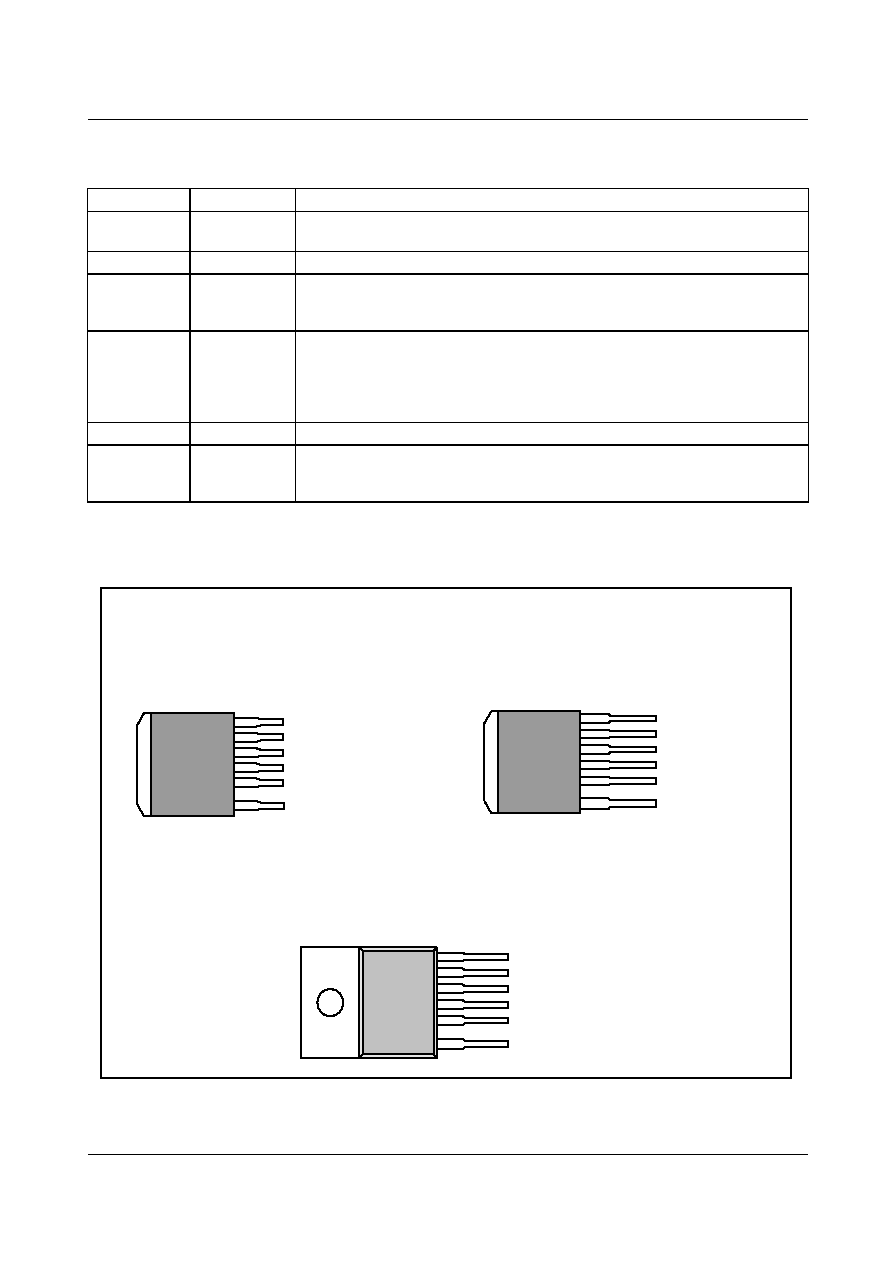
Pin Definitions
Pin Configuration
Figure 3. Pin Configuration (Top View)Absolute Maximum Ratings
Pin Number
Pin Name
Pin Function Description
1
Drain
This pin is the high voltage power SenseFET drain. It is designed to drive the
transformer directly.
2
GND
This pin is the control ground and the SenseFET source.
3
V
CC
This pin is the positive supply voltage input. Initially, During start up, the power is
supplied through the startup resistor from DC link. When Vcc reaches 12V, the
power is supplied from the auxiliary transformer winding.
4
Feedback (FB)
This pin is internally connected to the inverting input of the PWM comparator.
The collector of an optocoupler is typically tied to this pin. For stable operation, a
capacitor should be placed between this pin and GND. If the voltage of this pin
reaches 6.0V, the over load protection is activated resulting in shutdown of the
FPS.
5
N.C
.
This pin is not connected.
6
I_limit
This pin is for the pulse by pulse current limit level programming. By using a
resistor to GND on this pin, the current limit level can be changed. If this pin is
left floating, the typical current limit will be 3.0A.
FSC
M
0765
R
J
1 : Drain
2 : GND
6 : I_limit
4 : FB
3 : Vcc
5 : N.C.
D2-PAK-6L
FSCM
07
65RG
1. Drain
2. GND
3. Vcc
4. FB
6. I_limit
5. N.C.
TO-220-6L
FSCM0765RJ
FSCM0765RG
I2-PAK-6L
FSCM0765RI
FSCM0765RI
1 : Drain
2 : GND
6 : I_limit
4 : FB
3 : Vcc
5 : N.C.

FSCM0765R
4
(Ta=25
°
C, unless otherwise specified.)
Notes:
1. T
j
= 25
°
C to 150
°
C
2. Repetitive rating: Pulse width limited by maximum junction temperature
.
Thermal Impedance
Note:
1. Free standing with no heat-sink under natural convection
2. Infinite cooling condition - Refer to the SEMI G30-88.
Parameter
Symbol
Value
Unit
Drain-Source (GND) Voltage
(1)
V
DSS
650
V
Drain-Gate Voltage (R
GS
=1M
)
V
DGR
650
V
Gate-Source (GND) Voltage
V
GS
±
30
V
Drain Current Pulsed
(2)
I
DM
21
A
DC
Continuous Drain Current (D2-PAK, I2-PAK)
@ Tc = 25°C
I
D
5.3
A
DC
@ Tc =100
°
C
I
D
3.4
A
DC
Continuous Drain Current (TO-220)
@ Tc = 25°C
I
D
7
A
DC
@ Tc =100
°
C
I
D
4.4
A
DC
Supply Voltage
V
CC
20
V
Analog Input Voltage Range
V
FB
-0.3 to V
CC
V
Total Power Dissipation (D2-PAK,I2-PAK)
P
D
83
W
Total Power Dissipation (TO-220)
P
D
145
W
Operating Junction Temperature
T
J
Internally limited
°
C
Operating Ambient Temperature
T
A
-25 to +85
°
C
Storage Temperature Range
T
STG
-55 to +150
°
C
ESD Capability, HBM Model
(All pins except Vfb)
-
2.0
(GND-Vfb = 1.5kV)
(Vcc-Vfb = 1.0kV)
kV
ESD Capability, Machine Model
(All pins except Vfb)
-
300
(GND-Vfb = 250V)
(Vcc-Vfb = 100V)
V
Parameter
Symbol
Value
Unit
Junction-to-Ambient Thermal
JA
(1)
-
°
C/W
Junction-to-Case Thermal (D2-PAK, I2-PAK)
JC
(2)
1.5
°
C/W
Junction-to-Case Thermal (TO-220)
JC
(2)
0.9
°
C/W

FSCM0765R
5
Electrical Characteristics
(Ta = 25
°
C unless otherwise specified.)
Notes:
1. Pulse Test: Pulse width
300
S, duty
2%
2. These parameters, although guaranteed at the design, are not tested in mass production.
Parameter Symbol
Condition
Min.
Typ.
Max.
Unit
SenseFET SECTION
Drain Source Breakdown Voltage
BV
DSS
V
GS
= 0V, I
D
= 250
A
650
-
-
V
Zero-Gate-Voltage Current
I
DSS
V
DS
= Max, Rating
V
GS
= 0V
-
-
500
A
Static Drain Source on Resistance
(1)
R
DS(ON)
V
GS
= 10V, I
D
= 2.3A
-
1.4
1.6
Output Capacitance
C
OSS
V
GS
= 0V, V
DS
= 25V,
f = 1MHz
-
100
-
pF
Turn on Delay Time
T
D(ON)
V
DD
= 325V, I
D
= 5A
(MOSFET switching
time is essentially
independent of
operating temperature)
-
25
-
ns
Rise Time
T
R
-
60
-
Turn off Delay Time
T
D(OFF)
-
115
-
Fall Time
T
F
-
65
-
CONTROL SECTION
Initial Frequency
F
OSC
V
CC
= 14V, V
FB
= 5V
60
66
72
kHz
Modulated Frequency Range
F
mod
-
-
±3
-
kHz
Frequency Modulation Cycle
T
mod
-
-
4
-
ms
Voltage Stability
F
STABLE
10V
V
CC
17V
0
1
3
%
Temperature Stability
(2)
F
OSC
-
25
°
C
Ta
+85
°
C
-
±5
±10
%
Maximum Duty Cycle
D
MAX
-
75
80
85
%
Minimum Duty Cycle
D
MIN
-
-
-
0
%
Start Threshold Voltage
V
START
V
FB
= GND
11
12
13
V
Stop Threshold Voltage
V
STOP
V
FB
= GND
7
8
9
V
Feedback Source Current
I
FB
V
FB
= GND
0.7
0.9
1.1
mA
Soft-start Time
T
SS
-
10
15
20
ms
Initial Frequency
T
LEB
-
-
300
-
ns
BURST MODE SECTION
Burst Mode Voltages
(2)
V
BH
Vcc = 14V
0.4
0.5
0.6
V
VB
L
Vcc = 14V
0.24
0.3
0.36
V