 | ÐлекÑÑоннÑй компоненÑ: FSTU16862 | СкаÑаÑÑ:  PDF PDF  ZIP ZIP |
Äîêóìåíòàöèÿ è îïèñàíèÿ www.docs.chipfind.ru
© 2002 Fairchild Semiconductor Corporation
DS500703
www.fairchildsemi.com
May 2002
Revised May 2002
FSTU16
862 20
-Bi
t
B
u
s Swit
ch
w
i
th
-
2V Unde
rshoot
Pr
otect
ion
FSTU16862
20-Bit Bus Switch with
-
2V Undershoot Protection
General Description
The Fairchild Switch FSTU16862 provides 20-bits of high-
speed CMOS TTL-compatible bus switching. The low On
Resistance of the switch allows inputs to be connected to
outputs without adding propagation delay or generating
additional ground bounce noise.
The device is organized as a 20-bit bus switch. When OE
X
is LOW, the switch is ON and Port A is connected to Port B.
When OE
X
is HIGH, a high impedance state exists
between the A and B Ports. The A and B Ports are pro-
tected against undershoot to support an extended range to
2.0V below ground. Fairchild's integrated Undershoot
Hardened Circuit (UHC
) senses undershoot at the I/O
and responds by preventing voltage differentials from
developing and turning the switch on.
Features
s
Undershoot hardened to
-
2V (A and B Ports)
s
4
switch connection between two ports
s
Minimal propagation delay through the switch
s
Low l
CC
s
Zero bounce in flow-through mode
s
Control inputs compatible with TTL level
s
See Application Note AN-5008 for details on
FSTU - Undershoot Protected Fairchild Switch Family
Ordering Code:
Devices also available in Tape and Reel. Specify by appending the suffix letter "X" to the ordering code.
UHC
is a trademark of Fairchild Semiconductor Corporation.
Order Number
Package
Number
Package Description
FSTU16862QSP
MQA48A
48-Lead Quarter Size Very Small Outline Package (QVSOP), JEDEC MO-154, 0.150" Wide
FSTU16862MTD
MTD48
48-Lead Thin Shrink Small Outline Package (TSSOP), JEDEC MO-153, 6.1mm Wide
www.fairchildsemi.com
2
FSTU16862
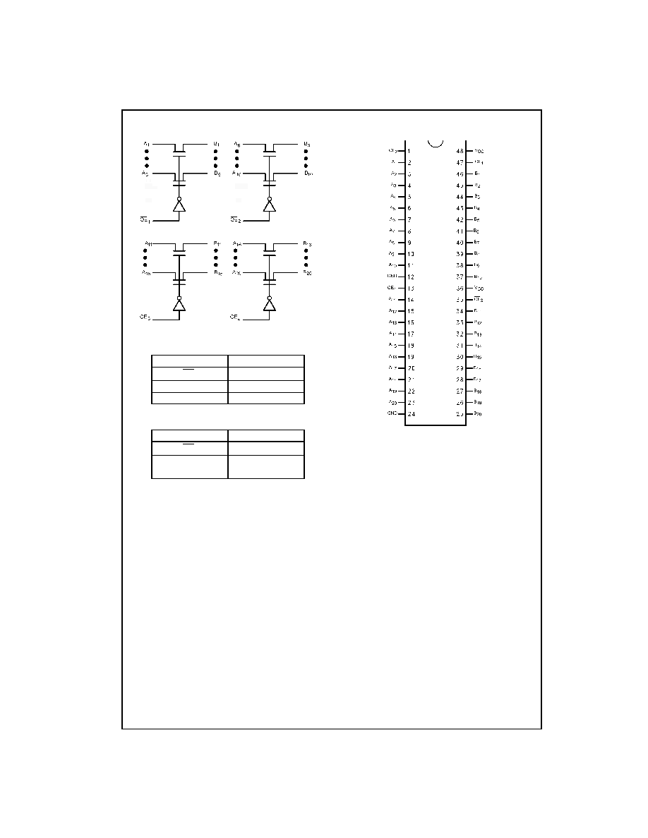
Logic Diagram
Pin Descriptions
Truth Table
H
=
HIGH Voltage Level
L
=
LOW Voltage Level
Z
=
High Impedance
Connection Diagram
Pin Name
Description
OE
x
Bus Switch Enables
A
Bus A
B
Bus B
Inputs
Inputs/Outputs
OE
x
A, B
L
A
=
B
H
Z
3
www.fairchildsemi.com
FSTU16
862
Absolute Maximum Ratings
(Note 1)
Recommended Operating
Conditions
(Note 4)
Note 1: The "Absolute Maximum Ratings" are those values beyond which
the safety of the device cannot be guaranteed. The device should not be
operated at these limits. The parametric values defined in the Electrical
Characteristics tables are not guaranteed at the absolute maximum rating.
The "Recommended Operating Conditions" table will define the conditions
for actual device operation.
Note 2: V
S
is the voltage observed/applied at either the A or B Ports across
the switch.
Note 3: The input and output negative voltage ratings may be exceeded if
the input and output diode current ratings are observed.
Note 4: Unused control inputs must be held HIGH or LOW. They may not
float.
DC Electrical Characteristics
Note 5: Typical values are at V
CC
=
5.0V and T
A
=
+
25
°
C
Note 6: Measured by the voltage drop between A and B pins at the indicated current through the switch. On Resistance is determined by the lower of the
voltages on the two (A or B) pins.
Note 7: Per TTL driven input, control pins only.
Supply Voltage (V
CC
)
-
0.5V to
+
7.0V
DC Switch Voltage (V
S
) (Note 2)
-
2.0V to
+
7.0V
DC Input Voltage (V
IN
) (Note 3)
-
0.5V to
+
7.0V
DC Input Diode Current (l
IK
) V
IN
<
0V
-
50 mA
DC Output Current (I
OUT
)
128 mA
DC V
CC
/GND Current (I
CC
/I
GND
)
±
100 mA
Storage Temperature Range (T
STG
)
-
65
°
C to
+
150
°
C
Power Supply Operating (V
CC)
4.0V to 5.5V
Input Voltage (V
IN
)
0V to 5.5V
Output Voltage (V
OUT
)
0V to 5.5V
Input Rise and Fall Time (t
r
, t
f
)
Switch Control Input
0 ns/V to 5 ns/V
Switch I/O
0 ns/V to DC
Free Air Operating Temperature (T
A
)
-40
°
C to
+
85
°
C
Symbol
Parameter
V
CC
T
A
=
-
40
°
C to
+
85
°
C
Units
Conditions
(V)
Min
Typ
(Note 5)
Max
V
IK
Clamp Diode Voltage
4.5
-
1.2
V
I
IN
=
-
18 mA
V
IH
HIGH Level Input Voltage
4.05.5
2.0
V
V
IL
LOW Level Input Voltage
4.05.5
0.8
V
I
I
Input Leakage Current
5.5
±
1.0
µ
A
0
V
IN
5.5V
0
10
µ
A
V
IN
=
5.5V
I
OZ
OFF-STATE Leakage Current
5.5
±
1.0
µ
A
0
A, B
V
CC
R
ON
Switch On Resistance
4.5
4
7
V
IN
=
0V, I
IN
=
64 mA
(Note 6)
4.5
4
7
V
IN
=
0V, I
IN
=
30 mA
4.5
8
14
V
IN
=
2.4V, I
IN
=
15 mA
4.0
11
20
V
IN
=
2.4V, I
IN
=
15 mA
I
CC
Quiescent Supply Current
5.5
3
µ
A
V
IN
=
V
CC
or GND, I
OUT
=
0
I
CC
Increase in I
CC
per Input
5.5
2.5
mA
One Input at 3.4V
(Note 7)
Other Inputs at V
CC
or GND
V
IKU
Voltage Undershoot
5.5
-
2.0
V
0.0 mA
I
IN
-
50 mA
OE
=
5.5V
www.fairchildsemi.com
4
FSTU16862
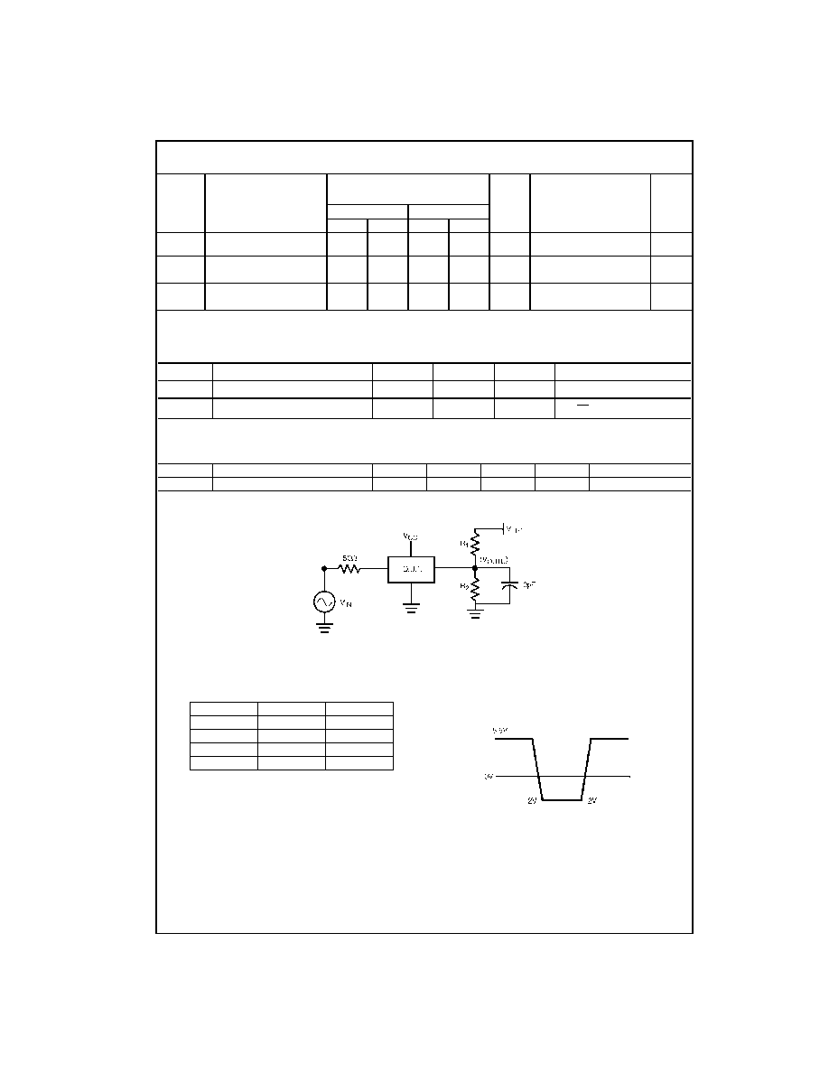
AC Electrical Characteristics
Note 8: This parameter is guaranteed by design but is not tested. The bus switch contributes no propagation delay other than the RC delay of the typical On
Resistance of the switch and the 50pF load capacitance, when driven by an ideal voltage source (zero output impedance).
Capacitance
(Note 9)
Note 9: T
A
=
+
25
°
C, f
=
1 MHz, Capacitance is characterized but not tested.
Undershoot Characteristic
(Note 10)
Note 10: This test is intended to characterize the device's protective capabilities by maintaining output signal integrity during an input transient voltage
undershoot event.
FIGURE 1.
Device Test Conditions
Transient
Input Voltage (V
IN
) Waveform
Symbol
Parameter
T
A
=
-
40
°
C to
+
85
°
C,
Units
Conditions
C
L
=
50pF, RU
=
RD
=
500
Figure
V
CC
=
4.5 5.5V
V
CC
=
4.0V
Number
Min
Max
Min
Max
t
PHL
, t
PLH
Propagation Delay Bus-to-Bus
(Note 8)
0.25
0.25
ns
V
I
=
OPEN
Figures
2, 3
t
PZH
, t
PZL
Output Enable Time
1.0
5.9
6.4
ns
V
I
=
7V for t
PZL
Figures
2, 3
V
I
=
OPEN for t
PZH
t
PHZ
, t
PLZ
Output Disable Time
1.0
6.9
7.4
ns
V
I
=
7V for t
PLZ
Figures
2, 3
V
I
=
OPEN for t
PHZ
Symbol
Parameter
Typ
Max
Units
Conditions
C
IN
Control Pin Input Capacitance
3
pF
V
CC
=
5.0V, V
IN
=
0V
C
I/O
Input/Output Capacitance "OFF State"
6
pF
V
CC
, OE
=
5.0V, V
IN
=
0V
Symbol
Parameter
Min
Typ
Max
Units
Conditions
V
OUTU
Output Voltage During Undershoot
2.5
V
OH
- 0.3
V
Figure 1
Parameter
Value
Units
V
IN
see Waveform
V
R
1
=
R
2
100K
V
TRI
11.0
V
V
CC
5.5
V
5
www.fairchildsemi.com
FSTU16
862
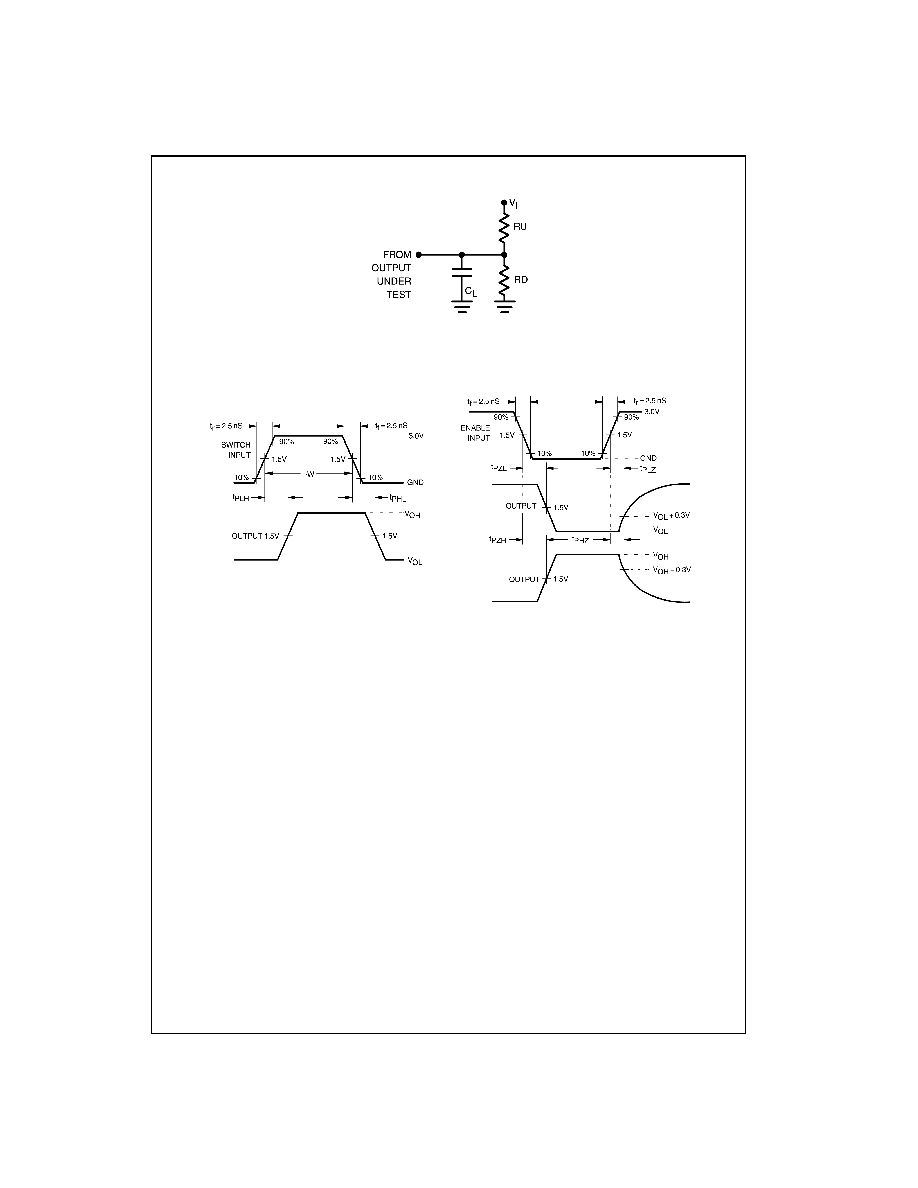
AC Loading and Waveforms
Note: Input driven by 50
source terminated in 50
Note: C
L
includes load and stray capacitance
Note: Input PRR
=
1.0 MHz, t
W
=
500 ns
FIGURE 2. AC Test Circuit
FIGURE 3. AC Waveforms