 | –≠–ª–µ–∫—Ç—Ä–æ–Ω–Ω—ã–π –∫–æ–º–ø–æ–Ω–µ–Ω—Ç: HCPL-0600 | –°–∫–∞—á–∞—Ç—å:  PDF PDF  ZIP ZIP |

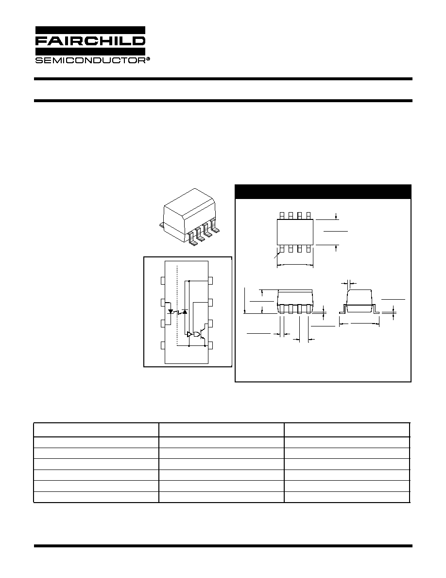
PACKAGE DIMENSIONS
4/10/03
Page 1 of 12
© 2003 Fairchild Semiconductor Corporation
HIGH SPEED-10 MBit/s
LOGIC GATE OPTOCOUPLERS
HCPL-0600
HCPL-0601
DESCRIPTION
The HCPL-0600/0601optocouplers consist of a 870 nm AlGaAS LED, optically coupled to a very high speed integrated photo-
detector logic gate with a strobable output. The devices are housed in a compact small-outline package. This output features an
open collector, thereby permitting wired OR outputs. The coupled parameters are guaranteed over the temperature range of -40∞C
to +85∞C. A maximum input signal of 5 mA will provide a minimum output sink current of 13 mA (fan out of 8). An internal noise
shield provides superior common mode rejection of typically 10 kV/µs.
FEATURES
∑
Compact SO8 package
∑
Very high speed-10 MBit/s
∑
Superior CMR-10 kV/µs
∑
Fan-out of 8 over -40∞C to +85∞C
∑
Logic gate output
∑
Strobable output
∑
Wired OR-open collector
∑
U.L. recognized (File # E90700)
APPLICATIONS
∑
Ground loop elimination
∑
LSTTL to TTL, LSTTL or
5-volt CMOS
∑
Line receiver, data transmission
∑
Data multiplexing
∑
Switching power supplies
∑
Pulse transformer replacement
∑
Computer-peripheral interface
TRUTH TABLE
(Positive Logic)
A 0.1 µF bypass capacitor must be connected between pins 8 and 5. (See note 1)
Input
Enable
Output
H
H
L
L
H
H
H
L
H
L
L
H
H
NC
L
L
NC
H
NOTE
All dimensions are in inches (millimeters)
Lead Coplanarity : 0.004 (0.10) MAX
0.202 (5.13)
Pin 1
0.019 (0.48)
0.182 (4.63)
0.021 (0.53)
0.011 (0.28)
0.050 (1.27)
TYP
0.244 (6.19)
0.224 (5.69)
0.143 (3.63)
0.123 (3.13)
0.008 (0.20)
0.003 (0.08)
0.010 (0.25)
0.006 (0.16)
SEATI
NG PLANE
0.164 (4.16)
0.144 (3.66)
1
2
3
4
5
6
7
8
N/C
_
V
CC
V
E
V
O
GND
+
N/C
V
F
Single-channel
circuit drawing

HIGH SPEED-10 MBit/s
LOGIC GATE OPTOCOUPLERS
HCPL-0600
HCPL-0601
4/10/03
Page 2 of 12
© 2003 Fairchild Semiconductor Corporation
*6.3 mA is a guard banded value which allows for at least 20% CTR degradation. Initial input current threshold value is 5.0 mA or
less
ABSOLUTE MAXIMUM RATINGS
(No derating required up to 85∞C)
Parameter
Symbol
Value
Units
Storage Temperature
T
STG
-55 to +125
∞C
Operating Temperature
T
OPR
-40 to +85
∞C
Lead Solder Temperature
T
SOL
260 for 10 sec
∞C
EMITTER
DC/Average Forward Input Current
I
F
50
mA
Enable Input Voltage
Not to exceed VCC by more than 500 mV
V
E
5.5
V
Reverse Input Voltage
V
R
5.0
V
Power Dissipation
P
I
45
mW
DETECTOR
Supply Voltage
V
CC
(1 minute max)
7.0 V
Output Current
I
O
50
mA
Output Voltage
V
O
7.0
V
Collector Output Power Dissipation
P
O
85
mW
RECOMMENDED OPERATING CONDITIONS
Parameter
Symbol
Min
Max
Units
Input Current, Low Level
I
FL
0
250
µA
Input Current, High Level
I
FH
*6.3
15
mA
Supply Voltage, Output
V
CC
4.5
5.5
V
Enable Voltage, Low Level
V
EL
0
0.8
V
Enable Voltage, High Level
V
EH
2.0
V
CC
V
Operating Temperature
T
A
-40
+85
∞C
Fan Out (TTL load)
N
8

4/10/03
Page 3 of 12
© 2003 Fairchild Semiconductor Corporation
HIGH SPEED-10 MBit/s
LOGIC GATE OPTOCOUPLERS
HCPL-0600
HCPL-0601
ELECTRICAL CHARACTERISTICS
(T
A
= -40∞C to +85∞C Unless otherwise specified.)
INDIVIDUAL COMPONENT CHARACTERISTICS
Parameter
Test Conditions
Symbol
Min
Typ**
Max
Unit
EMITTER
(I
F
= 10 mA)
V
F
1.8
V
Input Forward Voltage
T
A
=25∞C
1.75
Input Reverse Breakdown Voltage
(I
R
= 10 µA)
B
VR
5.0
V
Input Capacitance
(V
F
= 0, f = 1 MHz)
C
IN
60
pF
Input Diode Temperature Coefficient
(I
F
= 10 mA)
VF/
TA
-1.4
mV/∞C
DETECTOR
High Level Supply Current
(V
CC
= 5.5 V, I
F
= 0 mA)
(V
E
= 0.5 V)
I
CCH
7
10
mA
Low Level Supply Current
(V
CC
= 5.5 V, I
F
= 10 mA)
(V
E
= 0.5 V)
I
CCL
9
13
mA
Low Level Enable Current
(V
CC
= 5.5 V, V
E
= 0.5 V)
I
EL
-0.8
-1.6
mA
High Level Enable Current
(V
CC
= 5.5 V, V
E
= 2.0 V)
I
EH
-0.6
-1.6
mA
High Level Enable Voltage
(V
CC
= 5.5 V, I
F
= 10 mA)
V
EH
2.0
V
Low Level Enable Voltage
(V
CC
= 5.5 V, I
F
= 10 mA) (Note 2)
V
EL
0.8
V
SWITCHING CHARACTERISTICS
(T
A
= -40∞C to +85∞C, V
CC
= 5 V, I
F
= 7.5 mA Unless otherwise specified.)
AC Characteristics
Test Conditions
Device
Symbol
Min
Typ
Max
Unit
Propagation Delay Time
to Output High Level
(Note 3)
(T
A
=25∞C)
All
T
PLH
20
45
75
ns
(R
L
= 350
, C
L
= 15 pF) (Fig. 12)
100
Propagation Delay Time
to Output Low Level
(Note 4)
(T
A
=25∞C)
All
T
PHL
25
45
75
ns
(R
L
= 350
, C
L
= 15 pF) (Fig. 12)
100
Pulse Width Distortion
(R
L
= 350
, C
L
= 15 pF) (Fig. 12)
All
|T
PHL
-T
PLH
|
3
35
ns
Output Rise Time
(10-90%)
(R
L
= 350
, C
L
= 15 pF)
(Note 5) (Fig. 12)
All
t
r
50
ns
Output Fall Time
(90-10%)
(R
L
= 350
, C
L
= 15 pF)
(Note 6) (Fig. 12)
All
t
f
12
ns
Enable Propagation
Delay Time
to Output High Level
(I
F
= 7.5 mA, V
EH
= 3.5 V)
(R
L
= 350
, C
L
= 15 pF)
(Note 7) (Fig. 13)
All
t
ELH
20
ns
Enable Propagation
Delay Time
to Output Low Level
(I
F
= 7.5 mA, V
EH
= 3.5 V)
(R
L
= 350
, C
L
= 15 pF)
(Note 8) (Fig. 13)
All
t
EHL
20
ns
Common Mode
Transient Immunity
(at Output High Level)
(R
L
= 350
) (T
A
=25∞C)
(I
F
= 0 mA, V
OH
(Min.) = 2.0 V)
(Note 9)(Fig. 14)
|V
CM
| = 10 V HCPL-0600
|CM
H
|
10,000
V/µs
|V
CM
| = 50 V HCPL-0601
5000 10,000
Common Mode
Transient Immunity
(at Output Low Level)
(R
L
= 350
) (T
A
=25∞C)
(I
F
= 7.5 mA, V
OL
(Max.) = 0.8 V)
(Note 10)(Fig. 14)
|V
CM
| = 10 V HCPL-0600
|CM
H
|
10,000
V/µs
|V
CM
| = 50 V HCPL-0601
5000 10,000

HIGH SPEED-10 MBit/s
LOGIC GATE OPTOCOUPLERS
HCPL-0600
HCPL-0601
4/10/03
Page 4 of 12
© 2003 Fairchild Semiconductor Corporation
** All typical values are at V
CC
= 5 V, T
A
= 25∞C
1. The V
CC
supply to each optoisolator must be bypassed by a 0.1µF capacitor or larger. This can be either a ceramic or solid
tantalum capacitor with good high frequency characteristic and should be connected as close as possible to the package V
CC
and GND pins of each device.
2. Enable Input - No pull up resistor required as the device has an internal pull up resistor.
3. t
PLH
- Propagation delay is measured from the 3.75 mA level on the HIGH to LOW transition of the input current pulse to the
1.5V level on the LOW to HIGH transition of the output voltage pulse.
4. t
PHL
- Propagation delay is measured from the 3.75 mA level on the LOW to HIGH transition of the input current pulse to the
1.5V level on the HIGH to LOW transition of the output voltage pulse.
5. t
r
- Rise time is measured from the 90% to the 10% levels on the LOW to HIGH transition of the output pulse.
6. t
f
- Fall time is measured from the 10% to the 90% levels on the HIGH to LOW transition of the output pulse.
7. t
ELH
- Enable input propagation delay is measured from the 1.5V level on the HIGH to LOW transition of the input voltage pulse
to the 1.5V level on the LOW to HIGH transition of the output voltage pulse.
8. t
EHL
- Enable input propagation delay is measured from the 1.5V level on the LOW to HIGH transition of the input voltage pulse
to the 1.5V level on the HIGH to LOW transition of the output voltage pulse.
9. CM
H
- The maximum tolerable rate of rise of the common mode voltage to ensure the output will remain in the high state (i.e.,
V
OUT
> 2.0 V). Measured in volts per microsecond (V/µs).
10. CM
L
- The maximum tolerable rate of fall of the common mode voltage to ensure the output will remain in the low output state
(i.e., V
OUT
< 0.8 V). Measured in volts per microsecond (V/µs).
11. Device considered a two-terminal device: Pins 1,2,3 and 4 shorted together, and Pins 5,6,7 and 8 shorted together.
TRANSFER CHARACTERISTICS
(T
A
= -40∞C to +85∞C Unless otherwise specified.)
DC Characteristics
Test Conditions
Symbol
Min
Typ**
Max
Unit
High Level Output Current
(V
CC
= 5.5 V, V
O
= 5.5 V)
(I
F
= 250 µA, V
E
= 2.0 V) (Note 2)
I
OH
100
µA
Low Level Output Voltage
(V
CC
= 5.5 V, I
F
= 5 mA)
(V
E
= 2.0 V, I
OL
= 13 mA) (Note 2)
V
OL
.35
0.6
V
Input Threshold Current
(V
CC
= 5.5 V, V
O
= 0.6 V,
V
E
= 2.0 V, I
OL
= 13 mA)
I
FT
3
5
mA
ISOLATION CHARACTERISTICS
(T
A
= -40∞C to +85∞C Unless otherwise specified.)
Characteristics
Test Conditions
Symbol
Min
Typ**
Max
Unit
Input-Output
Insulation Leakage Current
(Relative humidity = 45%)
(T
A
= 25∞C, t = 5 s)
(V
I-O
= 3000 VDC)
(Note 11)
I
I-O
1.0*
µA
Withstand Insulation Test Voltage
(R
H
< 50%, T
A
= 25∞C)
(Note 11) ( t = 1 min.)
V
ISO
2500
V
RMS
Resistance (Input to Output)
(V
I-O
= 500 V) (Note 11)
R
I-O
10
12
Capacitance (Input to Output)
(f = 1 MHz) (Note 11)
C
I-O
0.6
pF
NOTES

4/10/03
Page 5 of 12
© 2003 Fairchild Semiconductor Corporation
HIGH SPEED-10 MBit/s
LOGIC GATE OPTOCOUPLERS
HCPL-0600
HCPL-0601
TYPICAL PERFORMANCE CURVES
Fig. 1 Forward Current vs. Input Forward Voltage
V
F
- FORWARD VOLTAGE (V)
1.100
1.200
1.300
1.400
1.500
1.600
I
F
- FOR
W
ARD CURRENT (mA)
0.01
0.1
1
10
100
1000
T
A
= 25∞C
Fig. 2 Output Voltage vs. Forward Current
I
OH
- HIGH LEVEL OUTPUT CURRENT (µA)
I
TH
- INPUT
THRESHOLD CURRENT (mA)
Fig. 3 Input Threshold Current vs. Temperature
T
A
- TEMPERATURE (∞C)
T
A
- TEMPERATURE (∞C)
-60
-40
-20
0
20
40
60
80
100
0
1
2
3
4
5
6
RL = 350
RL = 1 k
V
CC
= 5.0 V
V
O
= 0.6 V
Fig. 4 High Level Output Current vs. Temperature
-60
-40
-20
0
20
40
60
80
100
0
2
4
6
8
V
CC
= 5.5 V
V
O
= 5.5 V
V
E
= 2.0 V
I
F
= 250 µA
I
F
- FORWARD INPUT CURRENT (mA)
0
1
2
3
4
5
6
V
o
- OUTPUT
V
O
L
T
A
GE (V)
0
1
2
3
4
5
6
V
cc
= 5 V
T
A
= 25 ∞C
RL = 350
RL = 1 k


