
©2003 Fairchild Semiconductor Corporation
HUF76113SK8 Rev. B1
HUF76113SK8
6.5A, 30V, 0.030 Ohm, N-Channel, Logic
Level UltraFET Power MOSFET
This N-Channel power MOSFET is
manufactured using the innovative
UltraFETTM process. This advanced
process technology achieves the
lowest possible on-resistance per silicon area, resulting in
outstanding performance. This device is capable of
withstanding high energy in the avalanche mode and the
diode exhibits very low reverse recovery time and stored
charge. It was designed for use in applications where power
efficiency is important, such as switching regulators, switching
converters, motor drivers, relay drivers, low-voltage bus
switches, and power management in portable and battery-
operated products.
Formerly developmental type TA76113.
Features
∑ Logic Level Gate Drive
∑ 6.5A, 30V
∑ Ultra Low On-Resistance, r
DS(ON)
= 0.030
∑ Temperature Compensating PSPICE
Æ
Model
∑ Temperature Compensating SABERTM Model
∑ Thermal Impedance SPICE Model
∑ Thermal Impedance SABER Model
∑ Peak Current vs Pulse Width Curve
∑ UIS Rating Curve
∑ Related Literature
- TB334, "Guidelines for Soldering Surface Mount
Components to PC Boards"
Symbol
Packaging
JEDEC MS-012AA
Ordering Information
PART NUMBER
PACKAGE
BRAND
HUF76113SK8
MS-012AA
76113SK8
NOTE: When ordering, use the entire part number. Add the suffix T
to obtain the variant in tape and reel, e.g., HUF76113SK8T.
SOURCE(2)
DRAIN(8)
NC(1)
DRAIN(7)
DRAIN(6)
DRAIN(5)
SOURCE(3)
GATE(4)
BRANDING DASH
1
2
3
4
5
Data Sheet
January 2003

©2003 Fairchild Semiconductor Corporation
HUF76113SK8 Rev. B1
Absolute Maximum Ratings
T
A
= 25
o
C, Unless Otherwise Specified
HUF76113SK8
UNITS
Drain to Source Voltage (Note 1) . . . . . . . . . . . . . . . . . . . . . . . . . . . . . . . . . . . . . . . . . . V
DSS
30
V
Drain to Gate Voltage (R
GS
= 20k
) (Note 1) . . . . . . . . . . . . . . . . . . . . . . . . . . . . . . . . V
DGR
30
V
Gate to Source Voltage . . . . . . . . . . . . . . . . . . . . . . . . . . . . . . . . . . . . . . . . . . . . . . . . . . V
GS
±
20
V
Drain Current
Continuous (T
A
= 25
o
C, V
GS
= 10V) (Figure 2) (Note 2) . . . . . . . . . . . . . . . . . . . . . . . . . I
D
Continuous (T
A
= 100
o
C, V
GS
= 5V) (Note 3) . . . . . . . . . . . . . . . . . . . . . . . . . . . . . . . . . . I
D
Continuous (T
A
= 100
o
C, V
GS
= 4.5V) (Note 3) . . . . . . . . . . . . . . . . . . . . . . . . . . . . . . . . I
D
Pulsed Drain Current . . . . . . . . . . . . . . . . . . . . . . . . . . . . . . . . . . . . . . . . . . . . . . . . . . .I
DM
6.5
2.0
2.0
Figure 4
A
A
A
Pulsed Avalanche Rating . . . . . . . . . . . . . . . . . . . . . . . . . . . . . . . . . . . . . . . . . . . . . . . . E
ASB
Figure 6
Power Dissipation (Note 2) . . . . . . . . . . . . . . . . . . . . . . . . . . . . . . . . . . . . . . . . . . . . . . . . P
D
Derate Above 25
o
C . . . . . . . . . . . . . . . . . . . . . . . . . . . . . . . . . . . . . . . . . . . . . . . . . . . . . . .
2.5
20
W
mW/
o
C
Operating and Storage Temperature . . . . . . . . . . . . . . . . . . . . . . . . . . . . . . . . . . . . T
J
, T
STG
-55 to 150
o
C
Maximum Temperature for Soldering
Leads at 0.063in (1.6mm) from Case for 10s . . . . . . . . . . . . . . . . . . . . . . . . . . . . . . . . . . T
L
Package Body for 10s, See Techbrief 334 . . . . . . . . . . . . . . . . . . . . . . . . . . . . . . . . . . T
pkg
300
260
o
C
o
C
CAUTION: Stresses above those listed in "Absolute Maximum Ratings" may cause permanent damage to the device. This is a stress only rating and operation of the
device at these or any other conditions above those indicated in the operational sections of this specification is not implied.
NOTES:
1. T
J
= 25
o
C to 125
o
C.
2. 50
o
C/W measured using FR-4 board with 0.76 in
2
footprint at 10 seconds.
3. 177
o
C/W measured using FR-4 board with 0.0115 in
2
footprint at 1000 seconds.
Electrical Specifications
T
A
= 25
o
C, Unless Otherwise Specified
PARAMETER
SYMBOL
TEST CONDITIONS
MIN
TYP
MAX
UNITS
OFF STATE SPECIFICATIONS
Drain to Source Breakdown Voltage
BV
DSS
I
D
= 250
µ
A, V
GS
= 0V (Figure 12)
30
-
-
V
Zero Gate Voltage Drain Current
I
DSS
V
DS
= 25V, V
GS
= 0V
-
-
1
µ
A
V
DS
= 25V, V
GS
= 0V, T
A
= 150
o
C
-
-
250
µ
A
Gate to Source Leakage Current
I
GSS
V
GS
=
±
20V
-
-
±
100
nA
ON STATE SPECIFICATIONS
Gate to Source Threshold Voltage
V
GS(TH)
V
GS
= V
DS
, I
D
= 250
µ
A (Figure 11)
1
-
3
V
Drain to Source On Resistance
r
DS(ON)
I
D
= 6.5A, V
GS
= 10V (Figures 9, 10)
-
0.025
0.030
I
D
= 2.0A, V
GS
= 5V (Figure 9)
-
0.031
0.038
I
D
= 2.0A, V
GS
= 4.5V (Figure 9)
-
0.033
0.041
THERMAL SPECIFICATIONS
Thermal Resistance Junction to Ambient
R
JA
Pad Area = 0.76 in
2
(Note 2)
-
-
50
o
C/W
Pad Area = 0.054 in
2
(See TB337)
-
-
143
o
C/W
Pad Area = 0.0115 in
2
(See TB337)
-
-
177
o
C/W
SWITCHING SPECIFICATIONS (V
GS
= 4.5V)
Turn-On Time
t
ON
V
DD
= 15V, I
D
2.0A, R
L
= 7.5
,
V
GS
=
4.5V, R
GS
= 15
(Figure 15)
-
-
100
ns
Turn-On Delay Time
t
d(ON)
-
16
-
ns
Rise Time
t
r
-
50
-
ns
Turn-Off Delay Time
t
d(OFF)
-
28
-
ns
Fall Time
t
f
-
34
-
ns
Turn-Off Time
t
OFF
-
-
91
ns
HUF76113SK8

©2003 Fairchild Semiconductor Corporation
HUF76113SK8 Rev. B1
SWITCHING SPECIFICATIONS (V
GS
= 10V)
Turn-On Time
t
ON
V
DD
= 15V, I
D
6.5A, R
L
= 2.31
,
V
GS
=
10V, R
GS
= 16
(Figure 16)
-
-
59
ns
Turn-On Delay Time
t
d(ON)
-
6.5
-
ns
Rise Time
t
r
-
33
-
ns
Turn-Off Delay Time
t
d(OFF)
-
45
-
ns
Fall Time
t
f
-
40
-
ns
Turn-Off Time
t
OFF
-
-
126
ns
GATE CHARGE SPECIFICATIONS
Total Gate Charge
Q
g(TOT)
V
GS
= 0V to 10V
V
DD
= 15V, I
D
2.0A,
R
L
= 7.5
I
g(REF)
= 1.0mA
(Figures 14)
-
17.5
21
nC
Gate Charge at 5V
Q
g(5)
V
GS
= 0V to 5V
-
10
12
nC
Threshold Gate Charge
Q
g(TH)
V
GS
= 0V to 1V
-
0.65
0.78
nC
Gate to Source Gate Charge
Q
gs
-
1.10
-
nC
Gate to Drain "Miller" Charge
Q
gd
-
5.40
-
nC
CAPACITANCE SPECIFICATIONS
Input Capacitance
C
ISS
V
DS
= 25V, V
GS
= 0V, f = 1MHz
(Figure 13)
-
585
-
pF
Output Capacitance
C
OSS
-
327
-
pF
Reverse Transfer Capacitance
C
RSS
-
73
-
pF
Electrical Specifications
T
A
= 25
o
C, Unless Otherwise Specified
PARAMETER
SYMBOL
TEST CONDITIONS
MIN
TYP
MAX
UNITS
Source to Drain Diode Specifications
PARAMETER
SYMBOL
TEST CONDITIONS
MIN
TYP
MAX
UNITS
Source to Drain Diode Voltage
V
SD
I
SD
=6.5A
-
-
1.25
V
I
SD
= 2.0A
1.10
V
Reverse Recovery Time
t
rr
I
SD
= 2.0A, dI
SD
/dt = 100A/
µ
s
-
-
47
ns
Reverse Recovered Charge
Q
RR
I
SD
= 2.0A, dI
SD
/dt = 100A/
µ
s
-
-
52
nC
Typical Performance Curves
FIGURE 1. NORMALIZED POWER DISSIPATION vs AMBIENT
TEMPERATURE
FIGURE 2. MAXIMUM CONTINUOUS DRAIN CURRENT vs
AMBIENT TEMPERATURE
T
A
, AMBIENT TEMPERATURE (
o
C)
P
O
W
E
R DIS
S
IP
A
T
IO
N
M
U
L
T
IP
L
I
E
R
0
0
25
50
75
100
150
0.2
0.4
0.6
0.8
1.0
1.2
125
4
0
25
50
75
100
125
I
D
,
DRAIN CURRE
N
T
(
A
)
T
A
, AMBIENT TEMPERATURE (
o
C)
8
150
2
6
V
GS
= 4.5V, R
JA
= 177
o
C/W
V
GS
= 10V, R
JA
= 50
o
C/W
HUF76113SK8
©2003 Fairchild Semiconductor Corporation
HUF76113SK8 Rev. B1
FIGURE 3. NORMALIZED MAXIMUM TRANSIENT THERMAL IMPEDANCE
FIGURE 4. PEAK CURRENT CAPABILITY
FIGURE 5. FORWARD BIAS SAFE OPERATING AREA
NOTE: Refer to Fairchild Application Notes AN9321 and AN9322.
FIGURE 6. UNCLAMPED INDUCTIVE SWITCHING
CAPABILITY
Typical Performance Curves
(Continued)
t, RECTANGULAR PULSE DURATION (s)
10
-5
10
-1
10
0
10
0.01
1
10
-2
Z
JA
, NO
RM
A
L
IZ
E
D
T
H
E
R
M
A
L
IM
P
E
D
ANCE
0.001
10
-4
10
-3
SINGLE PULSE
NOTES:
DUTY FACTOR: D = t
1
/t
2
PEAK T
J
= P
DM
x Z
JA
x R
JA
+ T
A
P
DM
t
1
t
2
10
1
DUTY CYCLE - DESCENDING ORDER
0.5
0.2
0.1
0.05
0.01
0.02
0.1
10
2
10
3
R
JA
= 50
o
C/W
T
C
= 25
o
C
I
=
I
25
150 - T
A
125
FOR TEMPERATURES
ABOVE 25
o
C DERATE PEAK
CURRENT AS FOLLOWS:
V
GS
= 10V
TRANSCONDUCTANCE
MAY LIMIT CURRENT
IN THIS REGION
I
DM
, P
E
AK CURRE
NT
(
A
)
500
1
10
-5
10
-4
10
-3
10
-2
10
-1
10
0
10
3
t, PULSE WIDTH (s)
10
V
GS
= 5V
R
JA
= 50
o
C/W
100
10
2
10
1
T
J
= MAX RATED
T
A
= 25
o
C
100
µ
s
10ms
1ms
V
DSS(MAX)
= 30V
LIMITED BY r
DS(ON)
AREA MAY BE
OPERATION IN THIS
100
1
V
DS
, DRAIN TO SOURCE VOLTAGE (V)
1
100
500
10
I
D
, DRA
IN CURRE
NT
(
A
)
10
1
10
100
100
1
I
AS
, A
V
AL
ANCHE
CURRE
NT
(
A
)
t
AV
, TIME IN AVALANCHE (ms)
t
AV
= (L)(I
AS
)/(1.3*RATED BV
DSS
- V
DD
)
If R = 0
If R
0
t
AV
= (L/R)ln[(I
AS
*R)/(1.3*RATED BV
DSS
- V
DD
) +1]
STARTING T
J
= 25
o
C
STARTING T
J
= 150
o
C
0.1
10
0.01
HUF76113SK8

©2003 Fairchild Semiconductor Corporation
HUF76113SK8 Rev. B1
FIGURE 7. TRANSFER CHARACTERISTICS
FIGURE 8. SATURATION CHARACTERISTICS
FIGURE 9. DRAIN TO SOURCE ON RESISTANCE vs GATE
VOLTAGE AND DRAIN CURRENT
FIGURE 10. NORMALIZED DRAIN TO SOURCE ON
RESISTANCE vs JUNCTION TEMPERATURE
FIGURE 11. NORMALIZED GATE THRESHOLD VOLTAGE vs
JUNCTION TEMPERATURE
FIGURE 12. NORMALIZED DRAIN TO SOURCE BREAKDOWN
VOLTAGE vs JUNCTION TEMPERATURE
Typical Performance Curves
(Continued)
0
2
3
4
5
1
0
10
20
25
I
D,
DRAIN
CURRE
NT
(
A
)
V
GS
, GATE TO SOURCE VOLTAGE (V)
150
o
C
-55
o
C
25
o
C
PULSE DURATION = 80
µ
s
DUTY CYCLE = 0.5% MAX
V
DD
= 15V
30
15
5
0
10
0
1
2
3
20
I
D
, DRAIN
CURRE
NT
(
A
)
V
DS
, DRAIN TO SOURCE VOLTAGE (V)
30
5
15
4
I
D
, DRAIN
CURRE
NT
(
A
)
V
DS
, DRAIN TO SOURCE VOLTAGE (V)
PULSE DURATION = 80
µ
s
T
C
= 25
o
C
25
V
GS
= 3V
V
GS
= 3.5V
V
GS
= 4V
V
GS
= 5V
V
GS
= 4.5V
V
GS
= 10V
DUTY CYCLE = 0.5% MAX
50
100
150
0
4
V
GS
, GATE TO SOURCE VOLTAGE (V)
0
6
10
8
PULSE DURATION = 250
µ
s
r
DS
(
O
N)
, DRA
IN T
O
S
O
URCE
O
N
RE
S
I
S
T
ANCE
(
m
)
2
I
D
= 0.5A
I
D
= 2A
I
D
= 6.5A
DUTY CYCLE = 0.5% MAX
0.5
1.0
1.5
2.0
-80
-40
0
40
80
120
NO
RM
AL
IZ
E
D
DRAIN T
O
S
O
UR
CE
T
J
, JUNCTION TEMPERATURE (
o
C)
O
N
RE
S
I
S
T
ANCE
160
PULSE DURATION = 80
µ
s
V
GS
= 10V, I
D
= 6.5A
DUTY CYCLE = 0.5% MAX
-80
-40
0
40
80
120
0.6
0.7
0.8
1.0
1.2
NO
RM
AL
IZ
E
D
G
A
T
E
T
J
, JUNCTION TEMPERATURE (
o
C)
T
HRE
S
H
O
L
D V
O
L
T
A
G
E
V
GS
= V
DS
, I
D
= 250
µ
A
160
0.9
1.0
1.2
1.1
1.0
0.9
-80
-40
0
40
80
120
T
J
, JUNCTION TEMPERATURE (
o
C)
NO
RM
AL
IZ
E
D
DRAIN T
O
S
O
URCE
BRE
AKDO
W
N
V
O
L
T
A
G
E
I
D
= 250
µ
A
160
HUF76113SK8

©2003 Fairchild Semiconductor Corporation
HUF76113SK8 Rev. B1
FIGURE 13. CAPACITANCE vs DRAIN TO SOURCE VOLTAGE
NOTE: Refer to Fairchild Application Notes AN7254 and AN7260.
FIGURE 14. GATE CHARGE WAVEFORMS FOR CONSTANT
GATE CURRENT
FIGURE 15. SWITCHING TIME vs GATE RESISTANCE
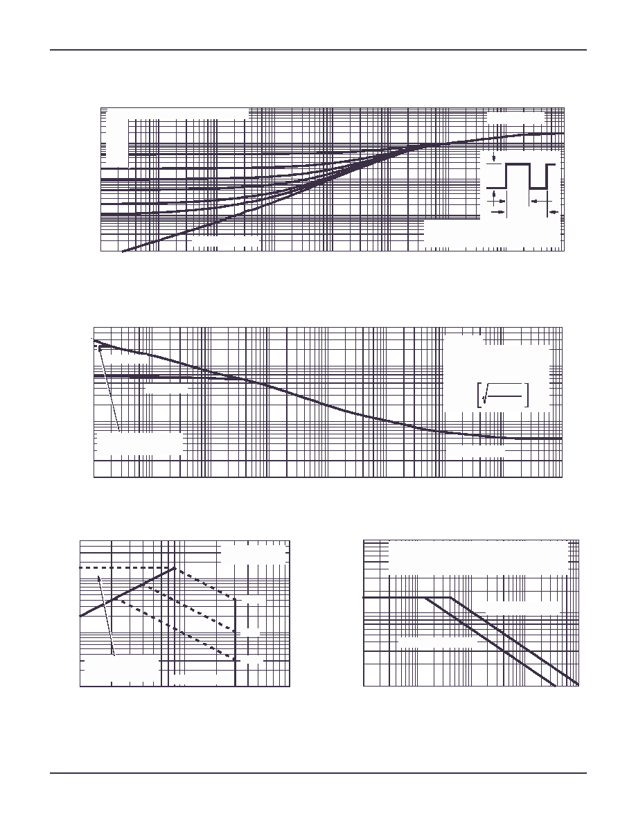
FIGURE 16. SWITCHING TIME vs GATE RESISTANCE
Test Circuits and Waveforms
FIGURE 17. UNCLAMPED ENERGY TEST CIRCUIT
FIGURE 18. UNCLAMPED ENERGY WAVEFORM
Typical Performance Curves
(Continued)
C
OSS
1200
800
0
0
5
15
25
C, CAP
A
C
IT
ANCE
(
p
F
)
1000
V
DS
, DRAIN TO SOURCE VOLTAGE (V)
600
30
400
C
ISS
C
RSS
10
20
200
V
GS
= 0V, f = 1MHz
C
ISS
= C
GS
+ C
GD
C
RSS
= C
GD
C
OSS
= C
DS
+ C
GD
10
8
6
4
0
V
GS
,
G
A
T
E
T
O
SO
U
R
C
E
V
O
L
T
A
G
E (
V
)
V
DD
= 15V
2
15
20
0
Q
g
, GATE CHARGE (nC)
5
I
D
= 6.5A
I
D
= 2.0A
I
D
= 0.5A
WAVEFORMS IN
DESCENDING ORDER:
10
30
20
30
40
50
0
120
90
60
0
10
S
W
IT
CHING
T
I
M
E
(
n
s
)
R
GS
, GATE TO SOURCE RESISTANCE (
)
t
d(OFF)
t
d(ON)
t
r
t
f
V
GS
= 4.5V, V
DD
= 15V, I
D
= 2A, R
L
= 7.5
60
20
30
40
50
0
150
120
90
0
10
S
W
IT
CHING
T
I
M
E
(
n
s
)
R
GS
, GATE TO SOURCE RESISTANCE (
)
t
d(OFF)
t
d(ON)
t
r
t
f
V
GS
= 10V, V
DD
= 15V, I
D
= 6.5A, R
L
= 2.31
30
t
P
V
GS
0.01
L
I
AS
+
-
V
DS
V
DD
R
G
DUT
VARY t
P
TO OBTAIN
REQUIRED PEAK I
AS
0V
V
DD
V
DS
BV
DSS
t
P
I
AS
t
AV
0
HUF76113SK8

©2003 Fairchild Semiconductor Corporation
HUF76113SK8 Rev. B1
Thermal Resistance vs. Mounting Pad Area
The maximum rated junction temperature, T
J(MAX)
, and the
thermal resistance of the heat dissipating path determines
the maximum allowable device power dissipation, P
D(MAX)
,
in an application. Therefore the application's ambient
temperature, T
A
(
o
C), and thermal resistance R
JA
(
o
C/W)
must be reviewed to ensure that T
J(MAX)
is never exceeded.
Equation 1 mathematically represents the relationship and
serves as the basis for establishing the rating of the part.
In using surface mount devices such as the SO-8 package,
the environment in which it is applied will have a significant
influence on the part's current and maximum power
dissipation ratings. Precise determination of the P
D(MAX)
is
complex and influenced by many factors:
1. Mounting pad area onto which the device is attached and
whether there is copper on one side or both sides of the
board
2. The number of copper layers and the thickness of the
board
3. The use of external heat sinks
4. The use of thermal vias
5. Air flow and board orientation
6. For non steady state applications, the pulse width, the
duty cycle and the transient thermal response of the part,
the board and the environment they are in.
Fairchild provides thermal information to assist the
designer's preliminary application evaluation. Figure 23
defines the R
JA
for the device as a function of the top
copper (component side) area. This is for a horizontally
FIGURE 19. GATE CHARGE TEST CIRCUIT
FIGURE 20. GATE CHARGE WAVEFORMS
FIGURE 21. SWITCHING TIME TEST CIRCUIT
FIGURE 22. SWITCHING TIME WAVEFORMS
Test Circuits and Waveforms
(Continued)
R
L
V
GS
+
-
V
DS
V
DD
DUT
I
g(REF)
V
DD
Q
g(TH)
V
GS
= 1V
Q
g(5)
V
GS
= 5V
Q
g(TOT)
V
GS
= 10
V
DS
V
GS
I
g(REF)
0
0
V
GS
R
L
R
GS
DUT
+
-
V
DD
V
DS
V
GS
t
ON
t
d(ON)
t
r
90%
10%
V
DS
90%
10%
t
f
t
d(OFF)
t
OFF
90%
50%
50%
10%
PULSE WIDTH
V
GS
0
0
(EQ. 1)
P
DMAX
T
JM AX
T
A
≠
(
)
Z
JA
----------------------------------------
=
HUF76113SK8

©2003 Fairchild Semiconductor Corporation
HUF76113SK8 Rev. B1
positioned FR-4 board with 1oz copper after 1000 seconds
of steady state power with no air flow. This graph provides
the necessary information for calculation of the steady state
junction temperature or power dissipation. Pulse applications
can be evaluated using the Fairchild device Spice thermal
model or manually utilizing the normalized maximum
transient thermal impedance curve.
Displayed on the curve are the three R
JA
values listed in
the Electrical Specifications table. The three points where
chosen to depict the compromise between the copper board
area, the thermal resistance and ultimately the power
dissipation, P
D(MAX)
. Thermal resistances corresponding to
other component side copper areas can be obtained from
Figure 23 or by calculation using Equation 2. The area, in
square inches is the top copper area including the gate and
source pads.
R
JA
(
o
C/W
)
50
100
150
200
AREA, TOP COPPER AREA (in
2
)
0.01
0.1
1.0
R
JA
= 79.3 - 21.8
*
ln(AREA)
143
o
C/W - 0.054in
2
177
o
C/W - 0.0115in
2
FIGURE 23. THERMAL RESISTANCE vs MOUNTING PAD AREA
0.001
250
(EQ. 2)
R
JA
79.3
21.8
Area
(
)
ln
◊
≠
=
HUF76113SK8

©2003 Fairchild Semiconductor Corporation
HUF76113SK8 Rev. B1
PSPICE Electrical Model
SUBCKT HUF76113SK8 2 1 3 ;
REV 4 June 1998
CA 12 8 9.60-10
CB 15 14 9.95e-10
CIN 6 8 5.01e-10
DBODY 7 5 DBODYMOD
DBREAK 5 11 DBREAKMOD
DPLCAP 10 5 DPLCAPMOD
EBREAK 11 7 17 18 32.3
EDS 14 8 5 8 1
EGS 13 8 6 8 1
ESG 6 10 6 8 1
EVTHRES 6 21 19 8 1
EVTEMP 20 6 18 22 1
IT 8 17 1
LDRAIN 2 5 1.00e-9
LGATE 1 9 1.00e-9
LSOURCE 3 7 2.27e-10
MMED 16 6 8 8 MMEDMOD
MSTRO 16 6 8 8 MSTROMOD
MWEAK 16 21 8 8 MWEAKMOD
RBREAK 17 18 RBREAKMOD 1
RDRAIN 50 16 RDRAINMOD 2.01e-3
RGATE 9 20 2.94
RLDRAIN 2 5 10
RLGATE 1 9 10
RLSOURCE 3 7 2.27
RSLC1 5 51 RSLCMOD 1e-6
RSLC2 5 50 1e3
RSOURCE 8 7 RSOURCEMOD 17.50e-3
RVTHRES 22 8 RVTHRESMOD 1
RVTEMP 18 19 RVTEMPMOD 1
S1A 6 12 13 8 S1AMOD
S1B 13 12 13 8 S1BMOD
S2A 6 15 14 13 S2AMOD
S2B 13 15 14 13 S2BMOD
VBAT 22 19 DC 1
ESLC 51 50 VALUE={(V(5,51)/ABS(V(5,51)))*(PWR(V(5,51)/(1e-6*180),2.5))}
.MODEL DBODYMOD D (IS = 9.35e-13 RS = 1.39e-2 TRS1 = 1.12e-6 TRS2 = 1.05e-6 CJO = 9.85e-10 TT = 2.82e-8 M = 0.42 )
.MODEL DBREAKMOD D (RS = 1.91e-1 TRS1 = 3.51e-3 TRS2 = 1.21e-6 )
.MODEL DPLCAPMOD D (CJO = 5.51e-10 IS = 1e-30 N = 10 M = 0.60 )
.MODEL MMEDMOD NMOS (VTO = 1.76 KP = 3.55 IS = 1e-30 N = 10 TOX = 1 L = 1u W = 1u RG = 2.94)
.MODEL MSTROMOD NMOS (VTO = 2.08 KP = 37 IS = 1e-30 N = 10 TOX = 1 L = 1u W = 1u)
.MODEL MWEAKMOD NMOS (VTO = 1.48 KP = 0.095 IS = 1e-30 N = 10 TOX = 1 L = 1u W = 1u RG = 29.4 RS=0.1)
.MODEL RBREAKMOD RES (TC1 = 1.02e-3 TC2 = 1.10e-7)
.MODEL RDRAINMOD RES (TC1 = 4.05e-2 TC2 = 1.12e-4)
.MODEL RSLCMOD RES (TC1 = 9.92e-3 TC2 = -2.06e-5)
.MODEL RSOURCEMOD RES (TC1 = 0 TC2 = 0)
.MODEL RVTHRESMOD RES (TC1 = -1.87e-3 TC2 = -5.42e-6)
.MODEL RVTEMPMOD RES (TC1 = -1.12e-3 TC2 = 1.12e-6)
.MODEL S1AMOD VSWITCH (RON = 1e-5 ROFF = 0.1 VON = -7.00 VOFF= -1.55)
.MODEL S1BMOD VSWITCH (RON = 1e-5 ROFF = 0.1 VON = -1.55 VOFF= -7.00)
.MODEL S2AMOD VSWITCH (RON = 1e-5 ROFF = 0.1 VON = 0.00 VOFF= 1.05)
.MODEL S2BMOD VSWITCH (RON = 1e-5 ROFF = 0.1 VON = 1.05 VOFF= 0.00)
.ENDS
NOTE: For further discussion of the PSPICE model, consult A New PSPICE Sub-Circuit for the Power MOSFET Featuring Global
Temperature Options; IEEE Power Electronics Specialist Conference Records, 1991, written by William J. Hepp and C. Frank Wheatley.
18
22
+
-
6
8
+
-
5
51
+
-
19
8
+
-
17
18
6
8
+
-
5
8
+
-
RBREAK
RVTEMP
VBAT
RVTHRES
IT
17
18
19
22
12
13
15
S1A
S1B
S2A
S2B
CA
CB
EGS
EDS
14
8
13
8
14
13
MWEAK
EBREAK
DBODY
RSOURCE
SOURCE
11
7
3
LSOURCE
RLSOURCE
CIN
RDRAIN
EVTHRES
16
21
8
MMED
MSTRO
DRAIN
2
LDRAIN
RLDRAIN
DBREAK
DPLCAP
ESLC
RSLC1
10
5
51
50
RSLC2
1
GATE
RGATE
EVTEMP
9
ESG
LGATE
RLGATE
20
+
-
+
-
+
-
6
HUF76113SK8

©2003 Fairchild Semiconductor Corporation
HUF76113SK8 Rev. B1
SABER Electrical Model
nom temp=25 deg c HUF76113SK8 Ultrafet
REV 4 June 98
template huf76113sk8 n2,n1,n3
electrical n2,n1,n3
{
var i iscl
d..model dbodymod = (is=9.35e-13, cjo= 9.85e-10,tt=2.82e-8, m=0.42)
d..model dbreakmod = ()
d..model dplcapmod = (cjo=5.51e-10,is=1e-30,n=10,m=0.60)
m..model mmedmod = (type=_n,vto=1.76,kp=3.55,is=1e-30, tox=1)
m..model mstrongmod = (type=_n,vto=2.08,kp=37,is=1e-30, tox=1)
m..model mweakmod = (type=_n,vto=1.48,kp=0.095,is=1e-30, tox=1)
sw_vcsp..model s1amod = (ron=1e-5,roff=0.1,von=-7.00,voff=-1.55)
sw_vcsp..model s1bmod = (ron=1e-5,roff=0.1,von=-1.55,voff=-7.00)
sw_vcsp..model s2amod = (ron=1e-5,roff=0.1,von=0,voff=1.05)
sw_vcsp..model s2bmod = (ron=1e-5,roff=0.1,von=1.05,voff=0)
c.ca n12 n8 = 9.60e-10
c.cb n15 n14 = 9.95e-10
c.cin n6 n8 = 5.01e-10
d.dbody n7 n71 = model=dbodymod
d.dbreak n72 n11 = model=dbreakmod
d.dplcap n10 n5 = model=dplcapmod
i.it n8 n17 = 1
l.ldrain n2 n5 = 1e-9
l.lgate n1 n9 = 1e-9
l.lsource n3 n7 = 2.27e-10
m.mmed n16 n6 n8 n8 = model=mmedmod, l=1u, w=1u
m.mstrong n16 n6 n8 n8 = model=mstrongmod, l=1u, w=1u
m.mweak n16 n21 n8 n8 = model=mweakmod, l=1u, w=1u
res.rbreak n17 n18 = 1, tc1=1.02e-3,tc2=1.10e-7
res.rdbody n71 n5 =1.39e-2, tc1=1.12e-6, tc2=1.05e-6
res.rdbreak n72 n5 =1.91e-1, tc1=3.51e-3, tc2=1.21e-6
res.rdrain n50 n16 = 2.01e-3, tc1=4.05e-2,tc2=1.12e-4
res.rgate n9 n20 = 2.94
res.rldrain n2 n5 = 10
res.rlgate n1 n9 = 10
res.rlsource n3 n7 = 2.27
res.rslc1 n5 n51 = 1e-6, tc1=-9.92e-3,tc2=-2.06e-5
res.rslc2 n5 n50 = 1e3
res.rsource n8 n7 = 17.5e-3, tc1=0,tc2=0
res.rvtemp n18 n19 = 1, tc1=-1.12e-3,tc2=1.12e-6
res.rvthres n22 n8 = 1, tc1=-1.87e-3,tc2=-5.42e-6
spe.ebreak n11 n7 n17 n18 = 32.3
spe.eds n14 n8 n5 n8 = 1
spe.egs n13 n8 n6 n8 = 1
spe.esg n6 n10 n6 n8 = 1
spe.evtemp n20 n6 n18 n22 = 1
spe.evthres n6 n21 n19 n8 = 1
sw_vcsp.s1a n6 n12 n13 n8 = model=s1amod
sw_vcsp.s1b n13 n12 n13 n8 = model=s1bmod
sw_vcsp.s2a n6 n15 n14 n13 = model=s2amod
sw_vcsp.s2b n13 n15 n14 n13 = model=s2bmod
v.vbat n22 n19 = dc=1
equations {
i (n51->n50) +=iscl
iscl: v(n51,n50) = ((v(n5,n51)/(1e-9+abs(v(n5,n51))))*((abs(v(n5,n51)*1e6/180))** 2.5 ))
}
}
18
22
+
-
6
8
+
-
19
8
+
-
17
18
6
8
+
-
5
8
+
-
RBREAK
RVTEMP
VBAT
RVTHRES
IT
17
18
19
22
12
13
15
S1A
S1B
S2A
S2B
CA
CB
EGS
EDS
14
8
13
8
14
13
MWEAK
EBREAK
DBODY
RSOURCE
SOURCE
11
7
3
LSOURCE
RLSOURCE
CIN
RDRAIN
EVTHRES
16
21
8
MMED
MSTRO
DRAIN
2
LDRAIN
RLDRAIN
DBREAK
DPLCAP
ISCL
RSLC1
10
5
51
50
RSLC2
1
GATE
RGATE
EVTEMP
9
ESG
LGATE
RLGATE
20
+
-
+
-
+
-
6
RDBODY
RDBREAK
72
71
HUF76113SK8

©2003 Fairchild Semiconductor Corporation
HUF76113SK8 Rev. B1
SPICE Thermal Model
(0.76 in
2
footprint)
REV 3 June 1998
HUF76113SK8
CTHERM1 th 6 3.75e-4
CTHERM2 6 5 3.05e-3
CTHERM3 5 4 3.70e-2
CTHERM4 4 3 2.52e-2
CTHERM5 3 2 8.50e-2
CTHERM6 2 tl 7.95e-1
RTHERM1 th 6 3.95e-2
RTHERM2 6 5 2.50e-1
RTHERM3 5 4 4.00e-1
RTHERM4 4 3 6.35
RTHERM5 3 2 2.02e1
RTHERM6 2 tl 4.80e1
SABER Thermal Model
(0.76 in
2
footprint)
SABER thermal model HUF76113SK8
template thermal_model th tl
thermal_c th, tl
{
ctherm.ctherm1 th 6 = 3.75e-4
ctherm.ctherm2 6 5 = 3.05e-3
ctherm.ctherm3 5 4 = 3.70e-2
ctherm.ctherm4 4 3 = 2.52e-2
ctherm.ctherm5 3 2 = 8.50e-2
ctherm.ctherm6 2 tl = 7.95e-1
rtherm.rtherm1 th 6 = 3.95e-2
rtherm.rtherm2 6 5 = 2.50e-1
rtherm.rtherm3 5 4 = 4.00e-1
rtherm.rtherm4 4 3 = 6.35
rtherm.rtherm5 3 2 = 2.02e1
rtherm.rtherm6 2 tl = 4.80e1
}
RTHERM4
RTHERM6
RTHERM5
RTHERM3
RTHERM2
RTHERM1
CTHERM4
CTHERM6
CTHERM5
CTHERM3
CTHERM2
CTHERM1
tl
2
3
4
5
6
th
JUNCTION
CASE
HUF76113SK8

Rev. I2
TRADEMARKS
The following are registered and unregistered trademarks Fairchild Semiconductor owns or is authorized to use and is not
intended to be an exhaustive list of all such trademarks.
DISCLAIMER
FAIRCHILD SEMICONDUCTOR RESERVES THE RIGHT TO MAKE CHANGES WITHOUT FURTHER NOTICE TO ANY
PRODUCTS HEREIN TO IMPROVE RELIABILITY, FUNCTION OR DESIGN. FAIRCHILD DOES NOT ASSUME ANY
LIABILITY ARISING OUT OF THE APPLICATION OR USE OF ANY PRODUCT OR CIRCUIT DESCRIBED HEREIN;
NEITHER DOES IT CONVEY ANY LICENSE UNDER ITS PATENT RIGHTS, NOR THE RIGHTS OF OTHERS.
LIFE SUPPORT POLICY
FAIRCHILD'S PRODUCTS ARE NOT AUTHORIZED FOR USE AS CRITICAL COMPONENTS IN LIFE SUPPORT
DEVICES OR SYSTEMS WITHOUT THE EXPRESS WRITTEN APPROVAL OF FAIRCHILD SEMICONDUCTOR
CORPORATION.
As used herein:
1. Life support devices or systems are devices or systems
which, (a) are intended for surgical implant into the body,
or (b) support or sustain life, or (c) whose failure to perform
when properly used in accordance with instructions for use
provided in the labeling, can be reasonably expected to
result in significant injury to the user.
2. A critical component is any component of a life support
device or system whose failure to perform can be
reasonably expected to cause the failure of the life support
device or system, or to affect its safety or effectiveness.
PRODUCT STATUS DEFINITIONS
Definition of Terms
ACExTM
ActiveArrayTM
BottomlessTM
CoolFETTM
CROSSVOLTTM
DOMETM
EcoSPARKTM
E
2
CMOSTM
EnSignaTM
FACTTM
FACT Quiet SeriesTM
FAST
Æ
FASTrTM
FRFETTM
GlobalOptoisolatorTM
GTOTM
HiSeCTM
I
2
CTM
ImpliedDisconnectTM
ISOPLANARTM
LittleFETTM
MicroFETTM
MicroPakTM
MICROWIRETM
MSXTM
MSXProTM
OCXTM
OCXProTM
OPTOLOGIC
Æ
OPTOPLANARTM
PACMANTM
POPTM
Power247TM
PowerTrench
Æ
QFETTM
QSTM
QT OptoelectronicsTM
Quiet SeriesTM
RapidConfigureTM
RapidConnectTM
SILENT SWITCHER
Æ
SMART STARTTM
SPMTM
StealthTM
SuperSOTTM-3
SuperSOTTM-6
SuperSOTTM-8
SyncFETTM
TinyLogic
Æ
TruTranslationTM
UHCTM
UltraFET
Æ
VCXTM
Across the board. Around the world.TM
The Power FranchiseTM
Programmable Active DroopTM
Datasheet Identification
Product Status
Definition
Advance Information
Formative or In
Design
This datasheet contains the design specifications for
product development. Specifications may change in
any manner without notice.
Preliminary
First Production
This datasheet contains preliminary data, and
supplementary data will be published at a later date.
Fairchild Semiconductor reserves the right to make
changes at any time without notice in order to improve
design.
No Identification Needed
Full Production
This datasheet contains final specifications. Fairchild
Semiconductor reserves the right to make changes at
any time without notice in order to improve design.
Obsolete
Not In Production
This datasheet contains specifications on a product
that has been discontinued by Fairchild semiconductor.
The datasheet is printed for reference information only.