 | ÐлекÑÑоннÑй компоненÑ: IRFI840A | СкаÑаÑÑ:  PDF PDF  ZIP ZIP |
Äîêóìåíòàöèÿ è îïèñàíèÿ www.docs.chipfind.ru
IRFW/I840A
BV
DSS
= 500 V
R
DS(on)
= 0.85
I
D
= 8 A
500
8
5.1
32
±
30
640
8
14.2
3.5
3.1
142
1.14
- 55 to +150
300
0.88
40
62.5
--
--
--
Avalanche Rugged Technology
Rugged Gate Oxide Technology
Lower Input Capacitance
Improved Gate Charge
Extended Safe Operating Area
Lower Leakage Current: 10
µ
A (Max.) @ V
DS
= 500V
Lower R
DS(ON)
: 0.638
(Typ.)
$GYDQFHG 3RZHU 026)(7
Thermal Resistance
Junction-to-Case
Junction-to-Ambient
Junction-to-Ambient
R
JC
R
JA
R
JA
°
C/W
Characteristic
Max.
Units
Symbol
Typ.
FEATURES
D
2
-PAK
1. Gate 2. Drain 3. Source
1
3
2
1
2
3
I
2
-PAK
*
*
When mounted on the minimum pad size recommended (PCB Mount).
Absolute Maximum Ratings
Drain-to-Source Voltage
Continuous Drain Current (T
C
=25
°
C)
Continuous Drain Current (T
C
=100
°
C)
Drain Current-Pulsed
(1)
Gate-to-Source Voltage
Single Pulsed Avalanche Energy
(2)
Avalanche Current
(1)
Repetitive Avalanche Energy
(1)
Peak Diode Recovery dv/dt
(3)
Total Power Dissipation (T
A
=25
°
C)
Total Power Dissipation (T
C
=25
°
C)
Linear Derating Factor
Operating Junction and
Storage Temperature Range
Maximum Lead Temp. for Soldering
Purposes, 1/8 from case for 5-seconds
Characteristic
Value
Units
Symbol
I
DM
V
GS
E
AS
I
AR
E
AR
dv/dt
P
D
I
D
T
J
, T
STG
T
L
A
V
mJ
A
mJ
V/ns
W
W
W/
°
C
A
°
C
V
DSS
V
*
©1999 Fairchild Semiconductor Corporation
Rev. B
IRFW/I840A
500
--
2.0
--
--
--
--
--
0.66
--
--
--
--
--
150
66
18
22
83
30
57
7.5
28.4
--
--
4.0
100
-100
10
100
0.85
--
1550
175
75
45
55
175
70
74
--
--
6.8
1190
--
--
--
370
3.9
8
32
1.4
--
--
Notes;
(1) Repetitive Rating: Pulse Width Limited by Maximum Junction Temperature
(2) L=18mH, I
AS
=8A, V
DD
=50V, R
G
=27
, Starting T
J
=25
°
C
(3) I
SD
8A, di/dt
160A/
µ
s, V
DD
BV
DSS
, Starting T
J
=25
°
C
(4) Pulse Test: Pulse Width = 250
µ
s, Duty Cycle
2%
(5) Essentially Independent of Operating Temperature
1&+$11(/
32:(5 026)(7
Electrical Characteristics
(T
C
=25
°
C unless otherwise specified)
Drain-Source Breakdown Voltage
Breakdown Voltage Temp. Coeff.
Gate Threshold Voltage
Gate-Source Leakage , Forward
Gate-Source Leakage , Reverse
Characteristic
Symbol
Max. Units
Typ.
Min.
Test Condition
Static Drain-Source
On-State Resistance
Forward Transconductance
Input Capacitance
Output Capacitance
Reverse Transfer Capacitance
Turn-On Delay Time
Rise Time
Turn-Off Delay Time
Fall Time
Total Gate Charge
Gate-Source Charge
Gate-Drain ( Miller ) Charge
g
fs
C
iss
C
oss
C
rss
t
d(on)
t
r
t
d(off)
t
f
Q
g
Q
gs
Q
gd
BV
DSS
BV/
T
J
V
GS(th)
R
DS(on)
I
GSS
I
DSS
V
V/
°
C
V
nA
µ
A
pF
ns
nC
--
--
--
--
--
--
--
--
--
--
--
--
--
V
GS
=0V,I
D
=250
µ
A
I
D
=250
µ
A
See Fig 7
V
DS
=5V,I
D
=250
µ
A
V
GS
=30V
V
GS
=-30V
V
DS
=500V
V
DS
=400V,T
C
=125
°
C
V
GS
=10V,I
D
=4A
(4)
V
DS
=50V,I
D
=4A
(4)
V
DD
=250V,I
D
=8A,
R
G
=9.1
See Fig 13
(4) (5)
V
DS
=400V,V
GS
=10V,
I
D
=8A
See Fig 6 & Fig 12
(4) (5)
Drain-to-Source Leakage Current
V
GS
=0V,V
DS
=25V,f =1MHz
See Fig 5
Source-Drain Diode Ratings and Characteristics
Continuous Source Current
Pulsed-Source Current
(1)
Diode Forward Voltage
(4)
Reverse Recovery Time
Reverse Recovery Charge
I
S
I
SM
V
SD
t
rr
Q
rr
Characteristic
Symbol
Max. Units
Typ.
Min.
Test Condition
--
--
--
--
--
A
V
ns
µ
C
Integral reverse pn-diode
in the MOSFET
T
J
=25
°
C,I
S
=8A,V
GS
=0V
T
J
=25
°
C,I
F
=8A
di
F
/dt=100A/
µ
s
(4)
IRFW/I840A
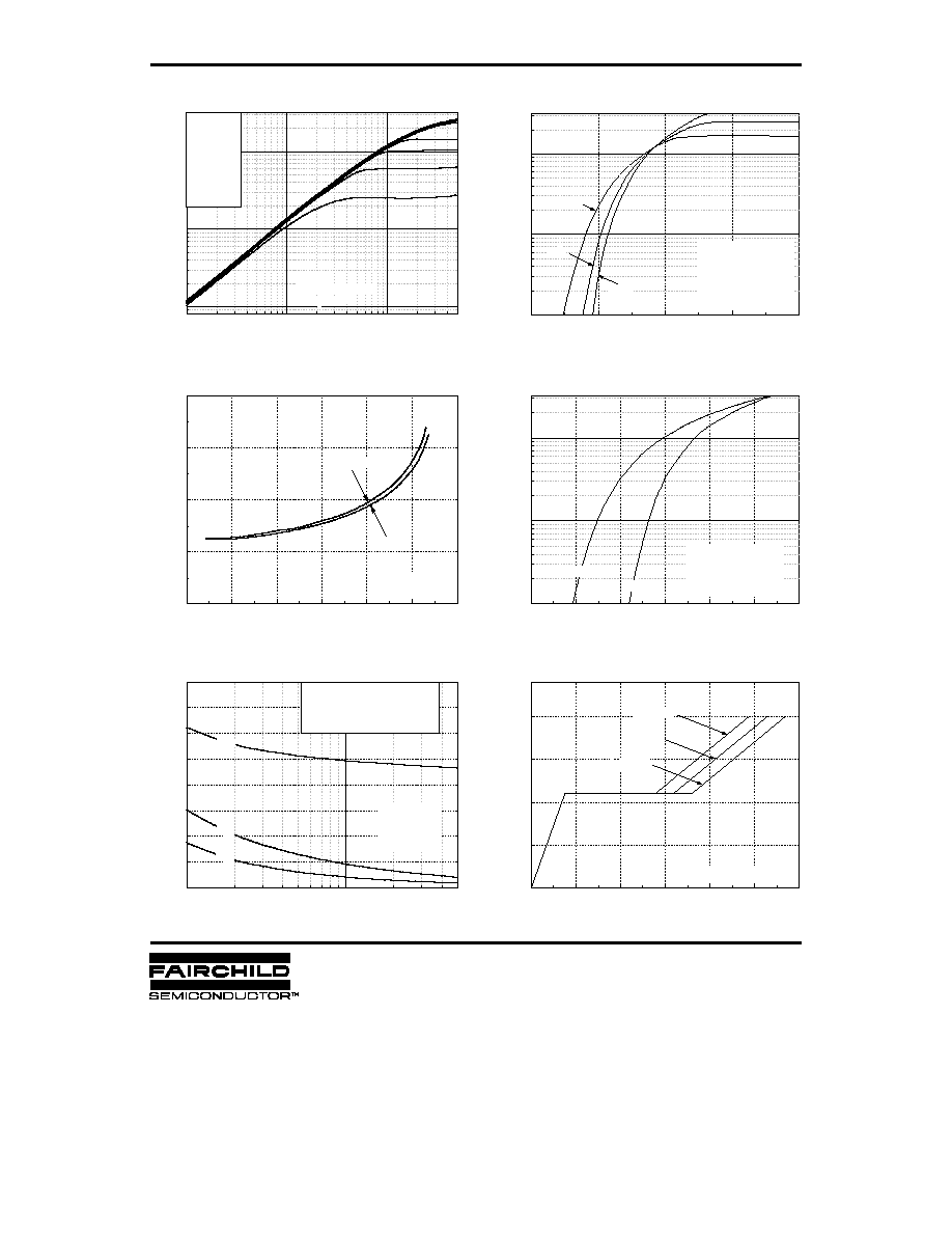
0
5
10
15
20
25
30
0.0
0.5
1.0
1.5
2.0
@ Note : T
J
= 25
o
C
V
GS
= 20 V
V
GS
= 10 V
R
DS(
on)
, [
]
Dr
ain-
Sour
ce O
n-Re
sis
tanc
e
I
D
, Drain Current [A]
0.2
0.4
0.6
0.8
1.0
1.2
1.4
10
-1
10
0
10
1
150
o
C
25
o
C
@ Notes :
1. V
GS
= 0 V
2. 250
µ
s Pulse Test
I
DR
,
R
eve
rs
e D
r
a
i
n
Cu
rr
ent
[A]
V
SD
, Source-Drain Voltage [V]
10
0
10
1
0
500
1000
1500
2000
C
iss
= C
gs
+ C
gd
(
C
ds
= shorted
)
C
oss
= C
ds
+ C
gd
C
rss
= C
gd
@ Notes :
1. V
GS
= 0 V
2. f = 1 MHz
C
rss
C
oss
C
iss
Ca
paci
tanc
e [
pF]
V
DS
, Drain-Source Voltage [V]
0
10
20
30
40
50
60
0
5
10
V
DS
= 400 V
V
DS
= 250 V
V
DS
= 100 V
@ Notes : I
D
= 8.0 A
V
GS
,
G
ate
-S
our
ce
V
olt
ag
e
[V
]
Q
G
, Total Gate Charge [nC]
10
-1
10
0
10
1
10
-1
10
0
10
1
@ Notes :
1. 250
µ
s Pulse Test
2. T
C
= 25
o
C
V
GS
Top : 1 5 V
1 0 V
8.0 V
7.0 V
6.0 V
5.5 V
5.0 V
Bottom : 4.5 V
I
D
,
Dra
in C
urre
nt
[A]
V
DS
, Drain-Source Voltage [V]
2
4
6
8
10
10
-1
10
0
10
1
25
o
C
150
o
C
- 55
o
C
@ Notes :
1. V
GS
= 0 V
2. V
DS
= 50 V
3. 250
µ
s Pulse Test
I
D
,
D
rai
n
Cur
re
nt
[
A
]
V
GS
, Gate-Source Voltage [V]
1&+$11(/
32:(5 026)(7
Fig 1. Output Characteristics
Fig 2. Transfer Characteristics
Fig 6. Gate Charge vs. Gate-Source Voltage
Fig 5. Capacitance vs. Drain-Source Voltage
Fig 4. Source-Drain Diode Forward Voltage
Fig 3. On-Resistance vs. Drain Current
IRFW/I840A
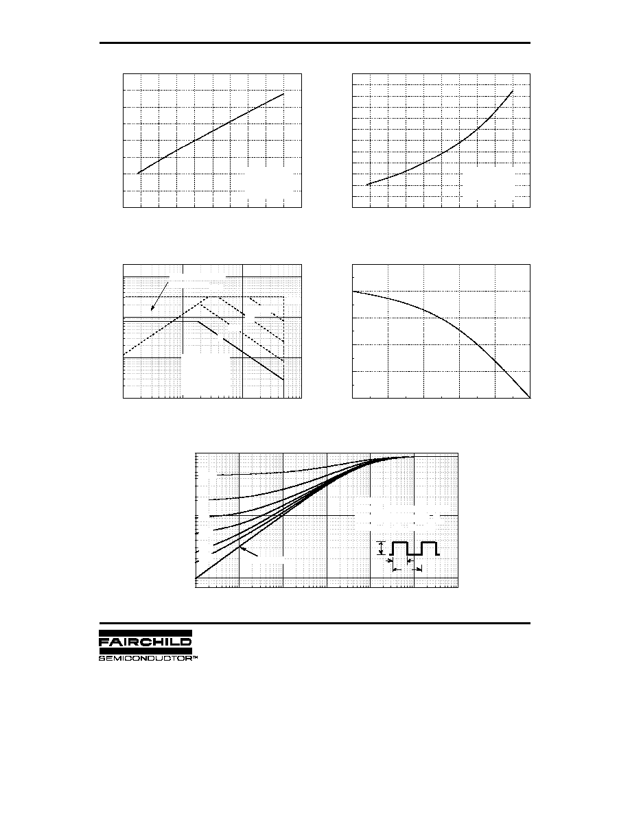
-75
-50
-25
0
25
50
75
100
125
150
175
0.8
0.9
1.0
1.1
1.2
@ Notes :
1. V
GS
= 0 V
2. I
D
= 250
µ
A
BV
DSS
,
(N
orm
ali
zed
)
Dr
ain
-So
urc
e B
reak
dow
n V
olt
age
T
J
, Junction Temperature [
o
C]
-75
-50
-25
0
25
50
75
100
125
150
175
0.0
0.5
1.0
1.5
2.0
2.5
3.0
@ Notes :
1. V
GS
= 10 V
2. I
D
= 4.0 A
R
DS
(on)
,
(N
or
mal
ize
d)
Dr
ain
-S
our
ce On-
Re
sis
tan
ce
T
J
, Junction Temperature [
o
C]
10
0
10
1
10
2
10
3
10
-1
10
0
10
1
10
2
DC
10
µ
s
100
µ
s
1 ms
10 ms
@ Notes :
1. T
C
= 25
o
C
2. T
J
= 150
o
C
3. Single Pulse
Operation in This Area
is Limited by R
DS(on)
I
D
,
Dr
ain
Cu
rre
nt
[A]
V
DS
, Drain-Source Voltage [V]
25
50
75
100
125
150
0
2
4
6
8
10
I
D
,
Dr
ai
n C
urr
ent
[A]
T
c
, Case Temperature [
o
C]
10
- 5
10
- 4
10
- 3
10
- 2
10
- 1
10
0
10
1
10
- 2
10
- 1
10
0
single pulse
0.2
0.1
0.01
0.02
0.05
D=0.5
@ Notes :
1. Z
J C
(t)=0.88
o
C/W Max.
2. Duty Factor, D=t
1
/t
2
3. T
J M
-T
C
=P
D M
*Z
J C
(t)
Z
JC
(t) ,
Thermal R
esponse
t
1
, Square Wave Pulse Duration [sec]
1&+$11(/
32:(5 026)(7
Fig 7. Breakdown Voltage vs. Temperature
Fig 8. On-Resistance vs. Temperature
Fig 11. Thermal Response
Fig 10. Max. Drain Current vs. Case Temperature
Fig 9. Max. Safe Operating Area
P
DM
t
1
t
2
IRFW/I840A
1&+$11(/
32:(5 026)(7
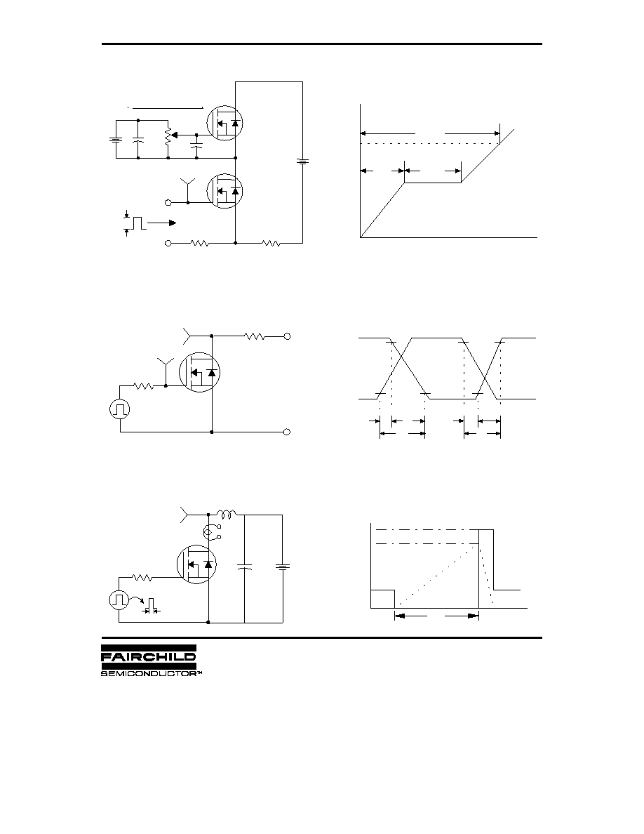
Fig 12. Gate Charge Test Circuit & Waveform
Fig 13. Resistive Switching Test Circuit & Waveforms
Fig 14. Unclamped Inductive Switching Test Circuit & Waveforms
E
AS
=
L
L
I
AS
2
----
2
1
--------------------
BV
DSS
-- V
DD
BV
DSS
V
in
V
out
10%
90%
t
d(on)
t
r
t
on
t
off
t
d(off)
t
f
Charge
V
GS
10V
Q
g
Q
gs
Q
gd
Vary t
p
to obtain
required peak I
D
10V
V
DD
C
L
L
V
DS
I
D
R
G
t
p
DUT
BV
DSS
t
p
V
DD
I
AS
V
DS
(t)
I
D
(t)
Time
V
DD
( 0.5 rated V
DS
)
10V
V
out
V
in
R
L
DUT
R
G
3mA
V
GS
Current Sampling (I
G
)
Resistor
Current Sampling (I
D
)
Resistor
DUT
V
DS
300nF
50k
200nF
12V
Same Type
as DUT
Current Regulator
R
1
R
2
Document Outline
- Main Menu
- Discrete Product Families
- MOSFETs
- Back
- Search
- fairchildsemi.com