 | ÐлекÑÑоннÑй компоненÑ: KA319 | СкаÑаÑÑ:  PDF PDF  ZIP ZIP |
Äîêóìåíòàöèÿ è îïèñàíèÿ www.docs.chipfind.ru
©2001 Fairchild Semiconductor Corporation
www.fairchildsemi.com
Rev. 1.0.2
Features
· Operates from a single 5V supply
· Typically 80ns response time at
±
15V
· Open collector outputs : up to + 35V
· High output drive current : 25mA
· Inputs and outputs can be isolated from system ground
· Minimum fan-out of 2 (each side)
· Two independent comparators
Description
The KA319 is a dual high speed voltage comparator
designed to operate from a single + 5V supply up to ±15V
dual supplies. Open collector of the output stage makes the
KA319 compatible with RTL, DTL and TTL as well as
capable of driving lamps and relays at currents up to
25mA. Typical response time of 80ns with ±15V power
supplies makes the KA319 ideal for application in fast A/D
converts, level shifters, oscillators, and multivibrators.
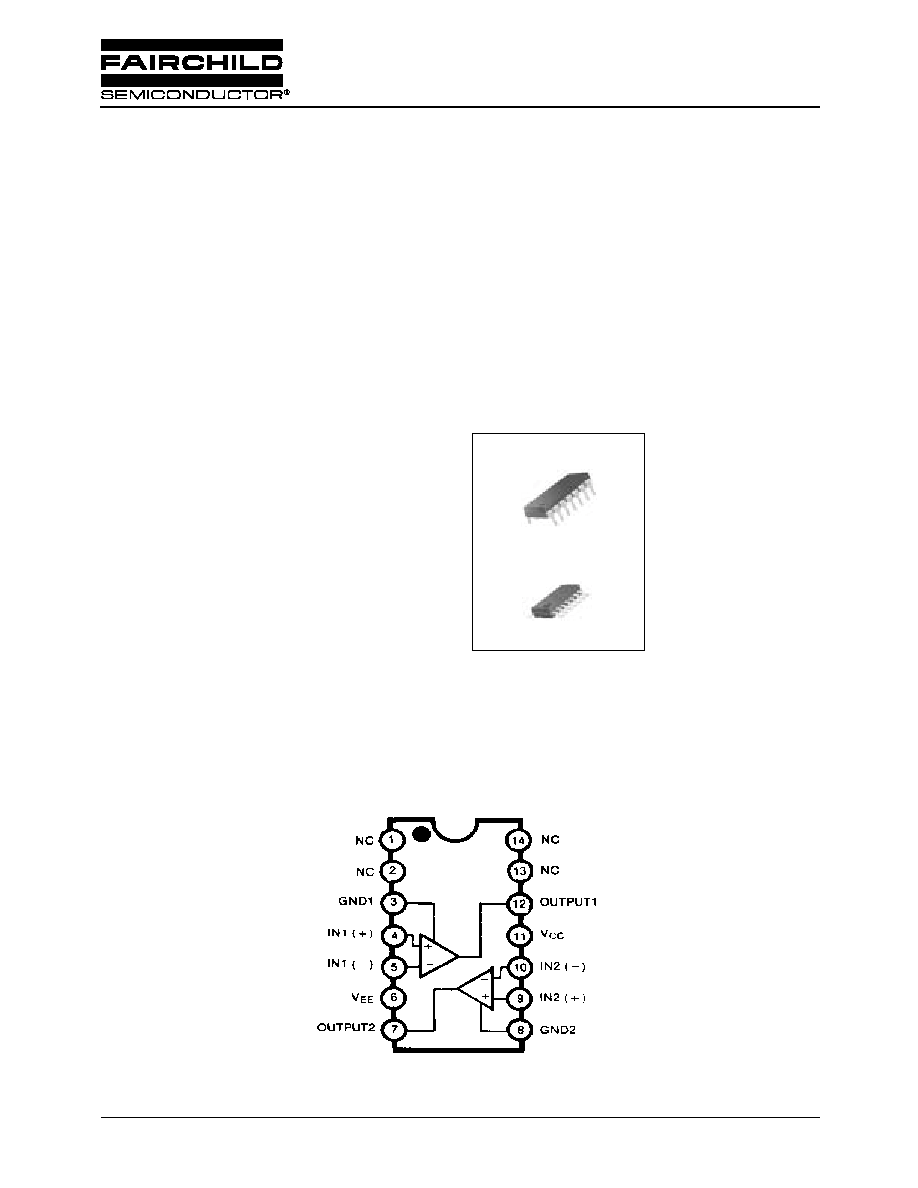
14-SOP
14-DIP
1
1
Internal Block Diagram
KA319
Dual Comparator
KA319
2
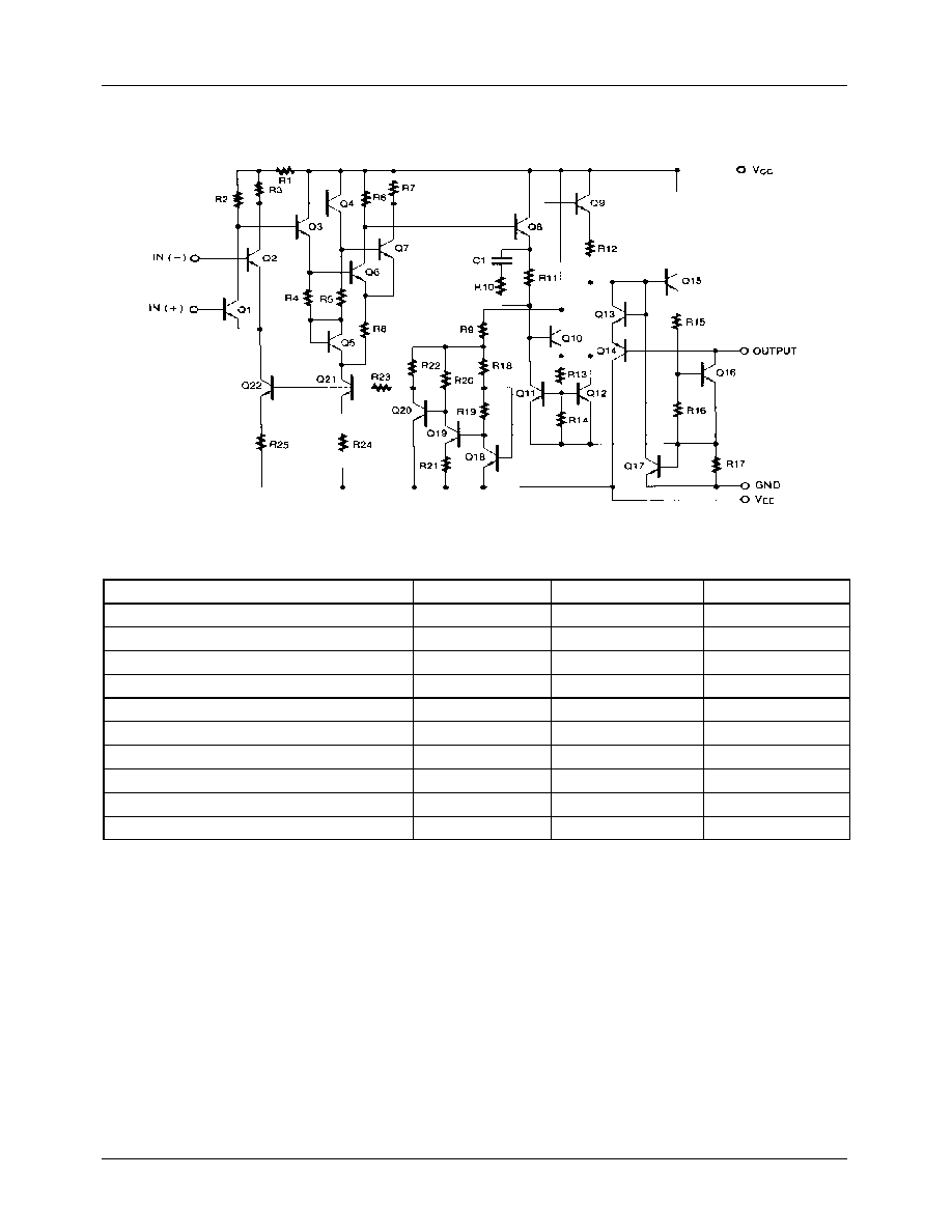
Schematic Diagram
Absolute Maximum Ratings
Parameter
Symbol
Value
Unit
Supply Voltage
V
CC
36
V
Output to Negative Supply Voltage
V
O
- V
EE
36
V
Ground to Negative Supply Voltage
V
EE
25
V
Ground to Positive Supply Voltage
V
CC
18
V
Differential Input Voltage
V
I(DIFF)
5
V
Input Voltage
V
I
±
15
V
Output Short Circuit Duration
-
10
sec
Power Dissipation
P
D
500
mW
Operating Temperature Range KA319
T
OPR
0 ~ + 70
°
C
Storage Temperature Range
T
STG
-65 ~ + 150
°
C
KA319
3
Electrical Characteristics
(V
CC
= +15V, V
EE
= -15V, T
A
= 25
°
C, unless otherwise specified)
Notes :
1. The offset voltage and offset currents given are the maximum values required to drive the output within a volt of either
supply with a 1mA load. Thus, these parameters define an error band and take into account the worst case effects of
voltage gain and input impedance.
2. The response time specified is for a 100mV input step with 5mV overdrive.
3. KA319 : 0
T
A
+70
°
C
Parameter
Symbol
Conditions
KA319
Unit
Min. Typ. Max.
Input Offset Voltage (Note 1)
V
IO
R
S
5K
-
2.0
8.0
mV
Note 3
-
-
10
Input Offset Current (Note 1)
I
IO
-
10
200
nA
Note 3
-
-
300
Input Bias Current
I
BIAS
-
150 1000
nA
Note 3
-
-
1200
Voltage Gain
G
V
-
8
40
-
V/mV
Response Time (Note 2)
T
RES
V
CC
=
±
15V
-
80
-
ns
Saturation Voltage
V
SAT
V
CC
=15V, V
EE
= -15V , V
I
-5mV, I
O
= 25mA
-
0.6
1.5
V
V
CC
= 4.5V,V
EE
= 0V
V
I
-10mV, I
O
3.2mA
Note3
-
0.3
0.4
Output Leakage Current
I
O(LKG)
V
I
5mV, V
O(P)
= 35V
-
-
-
µ
A
Note 3
-
-
-
V
I
10mV, V
O(P)
= 35V
-
0.2
10
Input Voltage Range
V
I(R)
Note 3
V
CC
=
±
15V
-
±
13
-
V
V
CC
= 5V, V
EE
= 0V
1
-
3
Differential Input Voltage
V
I(DIFF)
-
-
-
±
5
V
Positive Supply Current
I
CC1
V
CC
= 5V, V
EE
= 0V
-
3.6
-
mA
Positive Supply Current
I
CC2
V
CC
=
±
15V
-
7.5
12.5
mA
Negative Supply Current
I
EE
V
CC
=
±
15V
-
3
5
mA
KA319
4
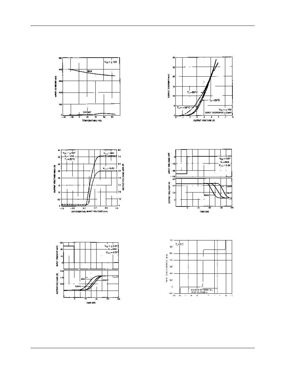
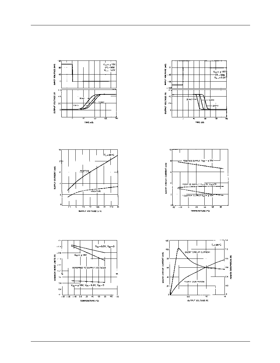
Typical Performance Characteristics
Figure 1. Input Current
Figure 2. Output Saturation Voltage
Figure 3. Transfer Function
Figure 4. Response Time for Various Input Overdriver
Figure 5. Response Time Various Input Overdriver
Figure 6. Input Characteristics
KA319
5
Typical Performance Characteristics (continued)
Figure 7. Response Time for Various Input Overdriver
Figure 8. Response Time for Various Input Overdriver
Figure 9. Supply Current
Figure 10. Supply Current
Figure 11. Common Mode Limits
Figure 12. Output Limiting Characteristics
KA319
6
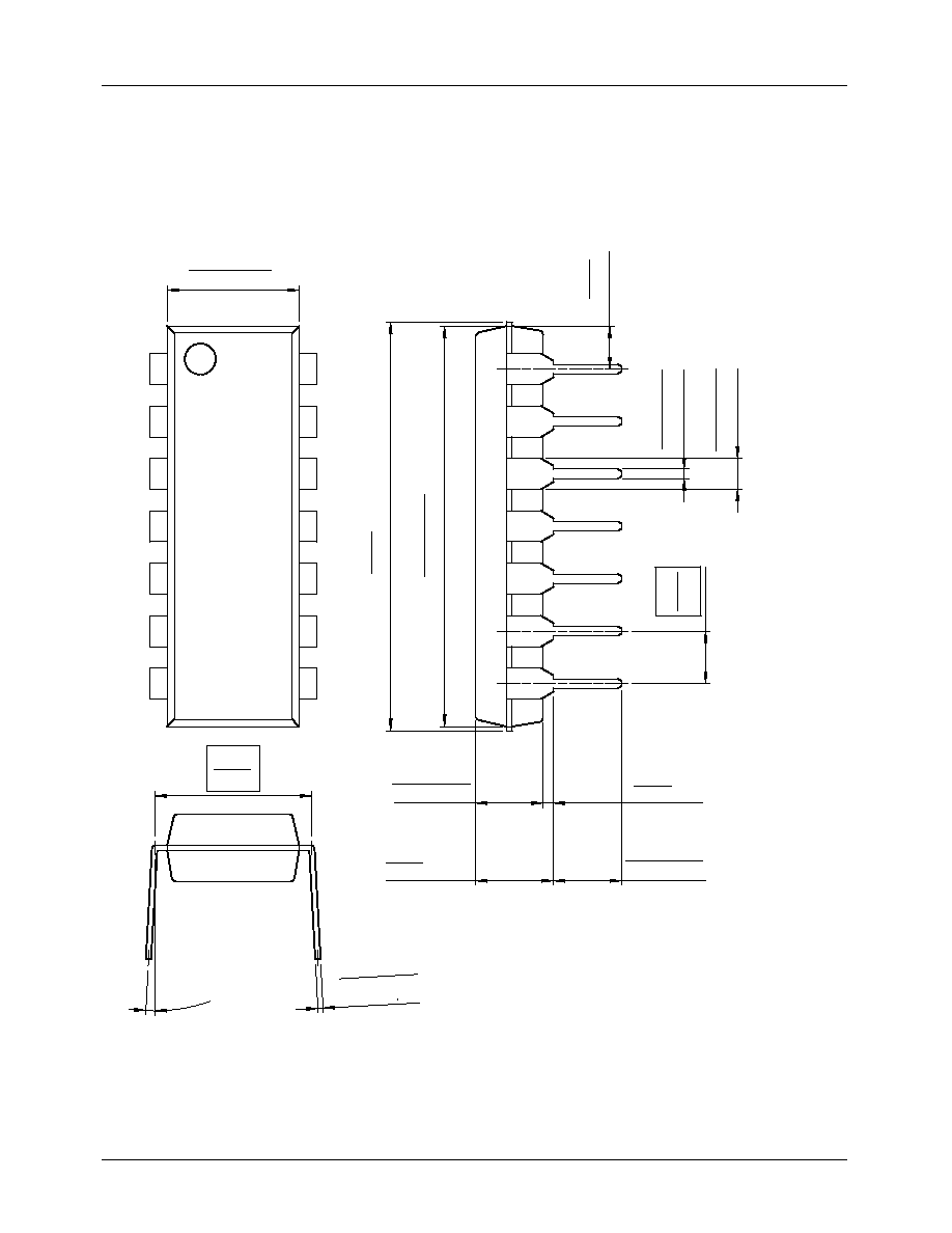
Mechanical Dimensions
Package
Dimensions in millimeters
6.40
±
0.20
7.62
0.300
2.54
0.100
#1
#7
#8
#14
0.252
±
0.008
0~15
°
0.25
+0.10
0.05
0.010
+0.004
0.002
3.30
±
0.30
0.130
±
0.012
3.25
±
0.20
0.128
±
0.008
19.40
±
0.20
0.764
±
0.008
19.80
0.780
MAX
5.08
0.200
0.20
0.008
MAX
MIN
2.08
0.082
()
0.46
±
0.10
0.018
±
0.004
0.059
±
0.004
1.50
±
0.10
14-DIP
KA319
7
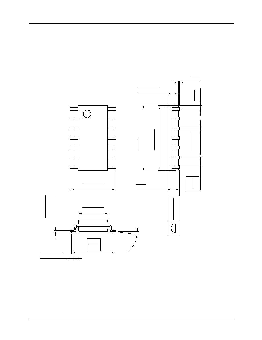
Mechanical Dimensions
(Continued)
Package
Dimensions in millimeters
8.56
±
0.20
0.337
±
0.008
1.27
0.050
5.72
0.225
1.55
±
0.10
0.061
±
0.004
0.05
0.002
6.00
±
0.30
0.236
±
0.012
3.95
±
0.20
0.156
±
0.008
0.60
±
0.20
0.024
±
0.008
8.70
0.343
MAX
#1
#7
#8
0~8
°
#14
0.47
0.019
()
1.80
0.071
MAX0.10
MAX0.004
MAX
MIN
+
0.10
-0.05
0.20
+
0.004
-0.002
0.008
+
0.10
-0.05
0.406
+
0.004
-0.002
0.016
14-SOP
KA319
8
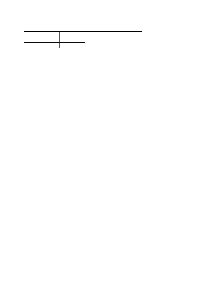
Ordering Information
Product Number
Package
Operating Temperature
KA319
14-DIP
0 ~ + 70
°
C
KA319D
14-SOP

KA319
9

KA319
10/22/01 0.0m 001
Stock#DSxxxxxxxx
2001 Fairchild Semiconductor Corporation
LIFE SUPPORT POLICY
FAIRCHILD'S PRODUCTS ARE NOT AUTHORIZED FOR USE AS CRITICAL COMPONENTS IN LIFE SUPPORT DEVICES
OR SYSTEMS WITHOUT THE EXPRESS WRITTEN APPROVAL OF THE PRESIDENT OF FAIRCHILD SEMICONDUCTOR
CORPORATION. As used herein:
1. Life support devices or systems are devices or systems
which, (a) are intended for surgical implant into the body,
or (b) support or sustain life, and (c) whose failure to
perform when properly used in accordance with
instructions for use provided in the labeling, can be
reasonably expected to result in a significant injury of the
user.
2. A critical component in any component of a life support
device or system whose failure to perform can be
reasonably expected to cause the failure of the life support
device or system, or to affect its safety or effectiveness.
www.fairchildsemi.com
DISCLAIMER
FAIRCHILD SEMICONDUCTOR RESERVES THE RIGHT TO MAKE CHANGES WITHOUT FURTHER NOTICE TO ANY
PRODUCTS HEREIN TO IMPROVE RELIABILITY, FUNCTION OR DESIGN. FAIRCHILD DOES NOT ASSUME ANY
LIABILITY ARISING OUT OF THE APPLICATION OR USE OF ANY PRODUCT OR CIRCUIT DESCRIBED HEREIN; NEITHER
DOES IT CONVEY ANY LICENSE UNDER ITS PATENT RIGHTS, NOR THE RIGHTS OF OTHERS.