 | –≠–ª–µ–∫—Ç—Ä–æ–Ω–Ω—ã–π –∫–æ–º–ø–æ–Ω–µ–Ω—Ç: KA4558 | –°–∫–∞—á–∞—Ç—å:  PDF PDF  ZIP ZIP |
©2001 Fairchild Semiconductor Corporation
www.fairchildsemi.com
Rev. 1.0.1
Features
∑ No frequency compensation required.
∑ No latch up.
∑ Large common mode and differential voltage range.
∑ Parameter tracking over temperature range.
∑ Gain and phase match between amplifiers.
∑ Internally frequency compensated.
∑ Low noise input transistors.
Descriptions
The KA4558 is a monolithic integrated circuit designed for
dual operational amplifier.
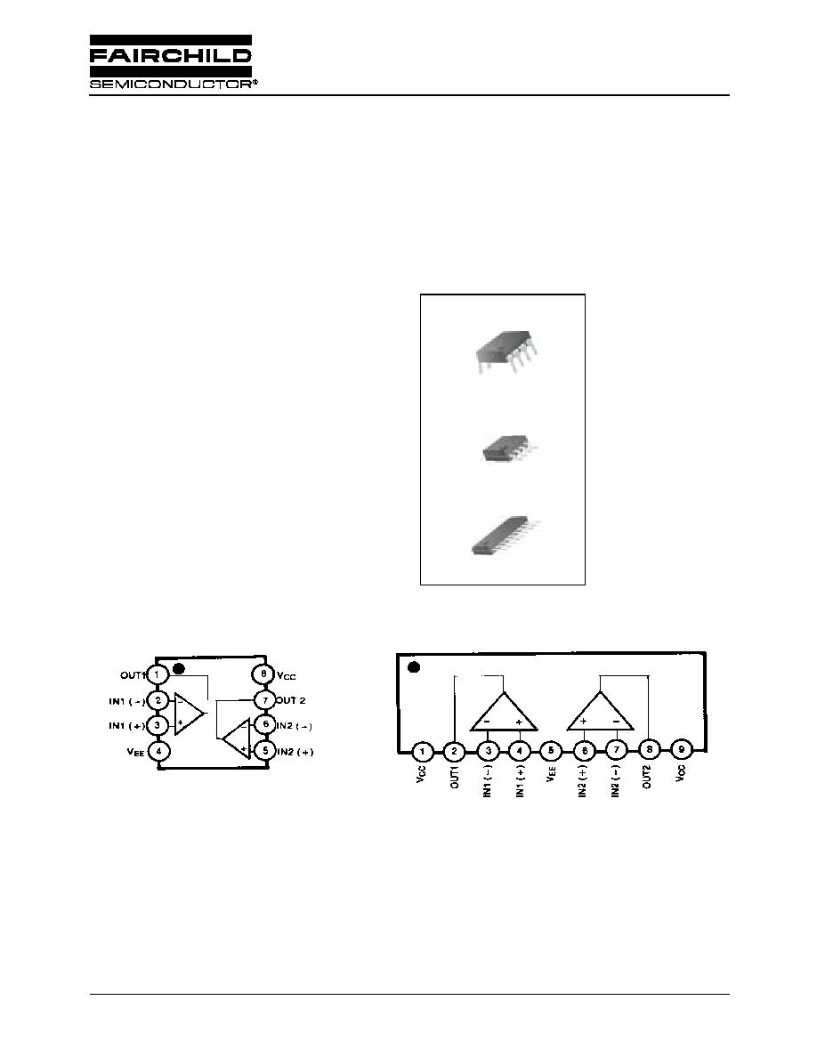
8-DIP
8-SOP
9-SIP
1
1
1
Internal Block Diagram
KA4558
Dual Operational Amplifier
KA4558
2
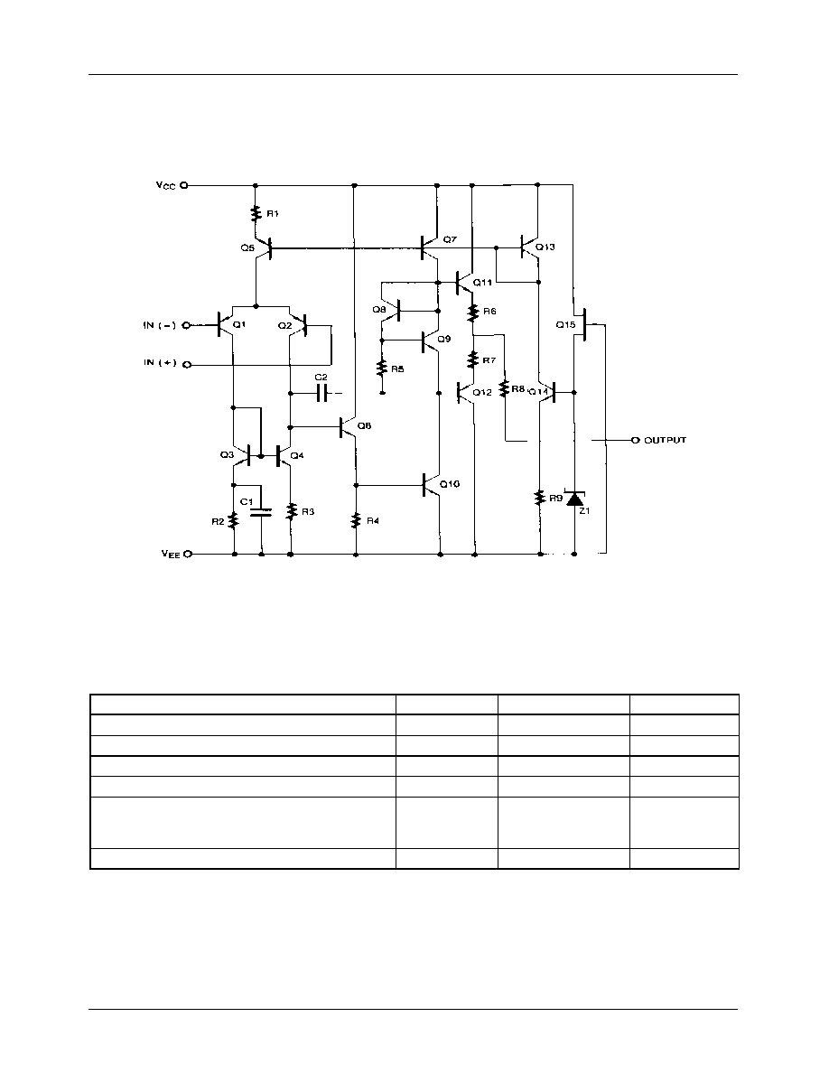
Schematic Diagram
(One Section Only)
Absolute Maximum Ratings
Parameter
Symbol
Value
Unit
Supply Voltage
V
CC
±
22
V
Differential Input Voltage
V
I(DIFF)
30
V
Input Voltage
V
I
±
15
V
Power Dissipation
P
D
400
mW
Operating Temperature Range
KA4558
KA4558I
T
OPR
0 ~ 70
-40 ~ 85
∞
C
Storage Temperature Range
T
STG
-65 ~ 150
∞
C

KA4558
3
Electrical Characteristics
(V
CC
= 15V, V
EE
= - 15V ,T
A
= 25
∞
C unless otherwise specified)
Note :
1. KA4558 : T
A(MIN)
T
A
T
A(MAX)
= 0
T
A
70
∞
C , KA4558I : T
A(MIN)
T
A
T
A(MAX)
= -40
T
A
+85
∞
C
2. Guaranteed by design.
Parameter Symbol
Conditions
KA4558/KA4558I
Unit
Min
Typ
Max
Input Offset Voltage
V
IO
R
S
10K
-
2
6
mV
Note 1
-
-
7.5
Input Offset Current
I
IO
-
5
200
nA
T
A
=T
A(MAX)
-
-
300
T
A
=T
A(MIN)
-
-
300
Input Bias Current
I
BIAS
-
30
500
nA
T
A
=T
A(MAX)
-
-
800
T
A
=T
A(MIN)
-
-
800
Large Signal
Voltage Gain
G
V
V
O(P-P)
=
±
10V,R
L
2K
20
200
-
V/mV
Note 1
-
-
-
Common Mode Input
Voltage Range
V
I(R)
±
12
±
13
-
V
Note 1
-
-
-
Common Mode
Rejection Ratio
CMRR
R
S
10K
70
90
-
dB
Note 1
-
-
-
Supply Voltage
Rejection Ratio
PSRR
R
S
10K
76
90
-
dB
Note 1
76
90
-
Output Voltage Swing
V
O(P-P)
R
L
10K
Note1
±
12
±
14
-
V
R
L
2K
±
10
±
13
-
Supply Current
(Both Amplifiers)
I
CC
-
3.5
5.8
mA
T
A
=T
A(MAX)
-
-
5.0
T
A
=T
A(MIN)
-
-
6.7
Power Consumption
(Both Amplifiers)
P
C
-
70
170
mW
T
A
=T
A(MAX)
-
-
150
T
a
= T
A(MIN)
-
-
200
Slew Rate (Note2)
SR
V
I
=10V, R
L
2K
C
I
100pF
1.2
-
-
V/
µ
s
Rise Time (Note2)
T
R
V
I
=20mV, R
L
2K
C
I
100pF
-
0.3
-
µ
s
Overshoot (Note2)
OS
V
I
=20mV, R
L
2K
C
I
100pF
-
15
-
%

KA4558
4
Typical Performance Characteristics
Figure 1. Burst Noise vs Source Resistance
Figure 2. RMS Noise vs Source Resistance
Figure 3. Output Noise vs Source Resistance
Figure 4. Spectral Noise Density
Figure 5. Open Loop Frequency Response
Figure 6. Phase Margin vs Frequency

KA4558
5
Typical Performance Characteristics (continued)
Figure 7. Positive Output Voltage Swing vs
Load Resistance
Figure 8. Negative Output Voltage Swing vs
Load Resistance
Figure 9. Power Bandwidth
(Large Signal Output Swing vs Frequency)

KA4558
6
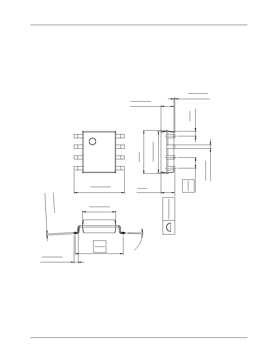
Mechanical Dimensions
Package
6.40
±
0.20
3.30
±
0.30
0.130
±
0.012
3.40
±
0.20
0.134
±
0.008
#1
#4
#5
#8
0.252
±
0.008
9.20
±
0.20
0.79
2.54
0.100
0.031
()
0.46
±
0.10
0.018
±
0.004
0.060
±
0.004
1.524
±
0.10
0.362
±
0.008
9.60
0.378
MAX
5.08
0.200
0.33
0.013
7.62
0~15
∞
0.300
MAX
MIN
0.25
+0.10
≠0.05
0.010
+0.004
≠0.002
8-DIP
KA4558
7
Mechanical Dimensions
(Continued)
Package
4.92
±
0.20
0.194
±
0.008
0.41
±
0.10
0.016
±
0.004
1.27
0.050
5.72
0.225
1.55
±
0.20
0.061
±
0.008
0.1~0.25
0.004~0.001
6.00
±
0.30
0.236
±
0.012
3.95
±
0.20
0.156
±
0.008
0.50
±
0.20
0.020
±
0.008
5.13
0.202
MAX
#1
#4
#5
0~8
∞
#8
0.56
0.022
()
1.80
0.071
MAX0.10
MAX0.004
MAX
MIN
+
0.10
-0.05
0.15
+
0.004
-0.002
0.006
8-SOP

KA4558
8
Mechanical Dimensions
(Continued)
Package
21.84
±
0.20
0.860
±
0.008
22.24
0.876
MAX
1.20
±
0.10
0.047
±
0.004
0.60
±
0.10
0.024
±
0.004
0.76
0.030
()
2.54
0.100
1.15
±
0.20
0.045
±
0.008
5.80
±
0.20
0.228
±
0.008
3.30
±
0.20
0.130
±
0.008
7.30
0.287
MAX
#1
#8
1.25
±
0.10
3.00
±
0.20
0.118
±
0.008
0.049
±
0.004
+
0.10
-0.05
6.00
0.236
MAX
0.25
+
0.004
-0.002
0.010
9-SIP

KA4558
9
Ordering Information
Product Number
Package
Operating Temperature
KA4558
8-DIP
0 ~ + 70
∞
C
KA4558D
8-SOP
KA4558S
9-SIP
KA4558I
8-DIP
-40 ~ + 85
∞
C

KA4558
6/1/01 0.0m 001
Stock#DSxxxxxxxx
2001 Fairchild Semiconductor Corporation
LIFE SUPPORT POLICY
FAIRCHILD'S PRODUCTS ARE NOT AUTHORIZED FOR USE AS CRITICAL COMPONENTS IN LIFE SUPPORT DEVICES
OR SYSTEMS WITHOUT THE EXPRESS WRITTEN APPROVAL OF THE PRESIDENT OF FAIRCHILD SEMICONDUCTOR
CORPORATION. As used herein:
1. Life support devices or systems are devices or systems
which, (a) are intended for surgical implant into the body,
or (b) support or sustain life, and (c) whose failure to
perform when properly used in accordance with
instructions for use provided in the labeling, can be
reasonably expected to result in a significant injury of the
user.
2. A critical component in any component of a life support
device or system whose failure to perform can be
reasonably expected to cause the failure of the life support
device or system, or to affect its safety or effectiveness.
www.fairchildsemi.com
DISCLAIMER
FAIRCHILD SEMICONDUCTOR RESERVES THE RIGHT TO MAKE CHANGES WITHOUT FURTHER NOTICE TO ANY
PRODUCTS HEREIN TO IMPROVE RELIABILITY, FUNCTION OR DESIGN. FAIRCHILD DOES NOT ASSUME ANY
LIABILITY ARISING OUT OF THE APPLICATION OR USE OF ANY PRODUCT OR CIRCUIT DESCRIBED HEREIN; NEITHER
DOES IT CONVEY ANY LICENSE UNDER ITS PATENT RIGHTS, NOR THE RIGHTS OF OTHERS.