 | –≠–ª–µ–∫—Ç—Ä–æ–Ω–Ω—ã–π –∫–æ–º–ø–æ–Ω–µ–Ω—Ç: KH300A | –°–∫–∞—á–∞—Ç—å:  PDF PDF  ZIP ZIP |

Features
I
-3dB bandwidth of 85MHz
I
3000V/
µsec slew rate
I
4ns rise and fall time
I
100mA output current
I
Low distortion, linear phase
Applications
I
Digital communications
I
Baseband and video communications
I
Instrument input/output amplifiers
I
Fast A to D, D to A conversion
I
Graphic CRT video drive amp
I
Coaxial cable line driver
General Description
The KH300 operational amplifier is a current feed-
back amplifier that provides a DC-85MHz -3dB band-
width that is virtually independent of gain setting.
Rise and fall times of 4ns and drive capability of
22V
pp
and 100mA add to the KH300's impressive
specifications.
Using the KH300 is as easy as adding power supplies
and a gain-setting resistor. Unlike conventional op
amp designs in which optimum gain-bandwidth
product occurs at a high gain, minimum settling time
at a gain of -1, maximum slew rate at a gain of +1,
et cetera, the KH300 offers consistent performance
at gain settings from 1 to 40 inverting or non-inverting.
As a result, designing with the KH300 is greatly
simplified. And since no external compensation is
necessary, "tweeks" on the production line have been
eliminated, making the KH300 an efficient
component for use in production situations.
Flat gain and phase response from DC to 45MHz and
superior rise and fall times make the KH300 an ideal
amplifier for a broad range of pulse, analog, and
digital applications. A 45MHz full power bandwidth
(20V
pp
into 100
) and 3000V/µsec slew rate eliminate
the need for power buffers in many applications
such as driving "flash" A to D converters or line-
driving. For applications requiring lower power
consumption, the KH300 can operate on supplies as
low as ±5V. Fast overload recovery (20ns) helps
prevent loss of data in communications applications
and flat phase response reduces distortion, even when
data must be sent over extended lengths of line.
The KH300A is packaged in a side-brazed 24-pin
ceramic DIP and is specified at 25∞C.
KH300
Wideband, High-Speed Operational Amplifier
www.fairchildsemi.com
REV. 1A February 2001
16
12
8
6
+
-
V
o
R
f
+V
CC
V+
V-
24
GND
13
-V
CC
1500
11
KH300 Equivalent Circuit Diagram
Pin 11 provides access to a 1500
feedback
resistor which can be connected to the out-
put or left open if an external feedback
resistor is desired. All undesignated pins are
internally unconnected.
2
REV. 1A February 2001
DATA SHEET
KH300
magnitude of gain {|V
out
/V
in
|]
4*
20
40
PARAMETERS
CONDITIONS TYP
MIN
2
TYP
MAX
2
TYP
UNITS
Frequency Domain Response
-3dB bandwidth
Vo < 4V
pp
105
75
85
70
MHz
Vo = 20V
pp
45
45
45
MHz
gain flatness
100KHz to 20MHz
±0.25
±0.08
±0.3
±0.25
dB
20MHz to 45MHz
±0.5
±0.25
±0.6
±1
dB
phase shift
1
1.6
2
deg/MHz
deviation from linear phase
DC to 45MHz
2
3
5
deg
reverse isolation
60
70
70
dB
distortion
refer to graphs
Time Domain Response
rise and fall time
5V output step
3
4
5
ns
20V output step
7
7
7
ns
settling time to 0.8%
10V output step
20
20
25
ns
overshoot (input rise time
1ns) 5V output step
5
5
5
%
slew rate
3
3
3
V/
µs
overload recovery (200% od)
< 50ns pulse width
20
20
20
ns
General Information
CONDITIONS MIN
2
TYP
MAX
2
UNITS
input offset voltage (drift)
10(25)
32
mV(
µV/∞C)
input bias current (drift)
non-inverting
10(20)
30
µV(nA/∞C)
inverting
30(50)
100
µV(nA/∞C)
equivalent input noise
1
integrated 0.1 to 100MHz,
22
56
µV
(R
s
= 50
, gain = 20)
second/third harmonic distortion 20MHz, +10dBm
48
38
-dBc
input impedance
non-inverting
100K/3
/pF
power supply rejection ratio
input referred
45
60
dB
common mode rejection ratio
input referred
64
dB
output drive voltage,current
10, 100
V, mA
supply current
24
33
mA
Min/max ratings are based on product characterization and simulation. Individual parameters are tested as noted. Outgoing quality levels are
determined from tested parameters.
NOTES:
1) For Noise Figure, refer to Distortion and Noise section in text.
2) 100% tested at +25∞C, A
V
= +20, R
L
= 100
, and V
CC
= ±15V.
* Refer to Low Gain Operation section.
Absolute Maximum Ratings
supply voltage (±V
CC
)
16V (±5V min)
output current (I
o
)
100mA
input voltage (V
imax
)
(|V
CC
| - 2.5)/A
V
common mode input voltage
±1/2 |V
CC
|
power dissipation
refer to graph
junction temperature (T
J
)
150∞C
storage temperature
-55∞C to +150∞C
still air thermal resistance (
ca
)
+25∞C/W
KH300 Electrical Characteristics
(25∞C, V
CC
= ±15V, R
L
= 100
; unless noted)
KH300
DATA SHEET
REV. 1A February 2001
3
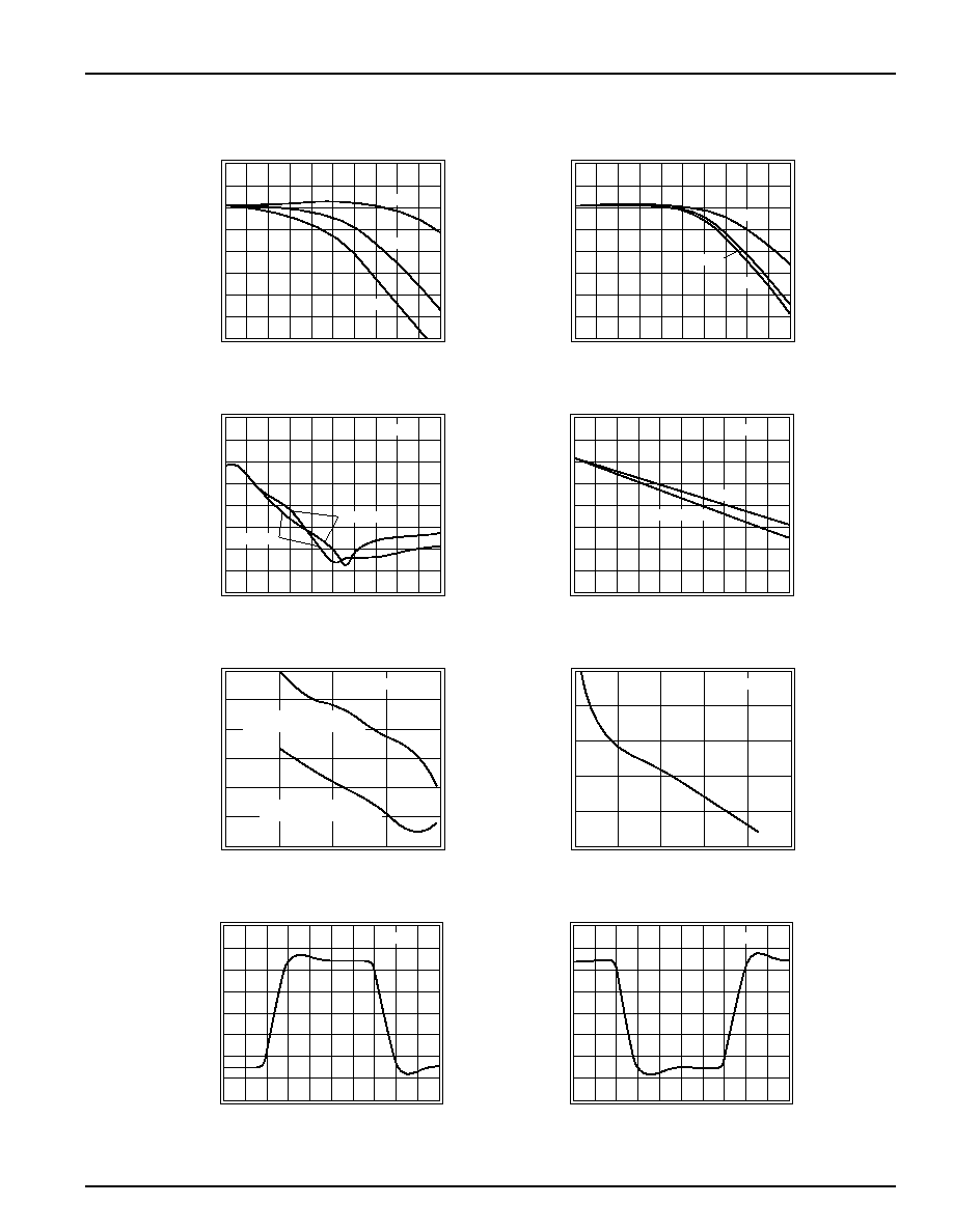
KH300 Performance Characteristics
(25∞C, V
CC
= ±15V, R
L
= 100
; unless noted)
Non-Inverting Gain
Relative Gain (1dB/div)
Freguency (MHz)
0
10
20
30
40
50
60
70
80
90
100
A
v
= 4
A
v
= 20
A
v
= 40
Inverting Gain
Relative Gain (1dB/div)
Freguency (MHz)
0
10
20
30
40
50
60
70
80
90
100
A
v
= 4
A
v
= 20
A
v
= 40
Broadband Inverting & Non-Inverting Gain
Relative Gain (10dB/div)
Freguency (MHz)
0
100 200 300 400 500 600 700 800 900 1GHz
Non-inverting
A
v
= 20
Inverting
Inverting & Non-Inverting Phase
Freguency (MHz)
0
10
20
30
40
50
60
70
80
90
100
Non-inverting
A
v
= 20
Inverting
-180
∞
-90
∞
0
∞
-360
∞
-270
∞
-180
∞
2nd & 3rd Harmonic Distortion Intercept
Intercept Point (+dBm)
Freguency (Hz)
10
4
10
5
10
6
10
7
10
8
(I
2
)
2nd harmonic intercept
exceeds 90dBm below 10
5
Hz
A
v
= 20
(I
3
)
3rd harmonic intercept
exceeds 64dBm below 10
5
Hz
30
40
50
60
70
80
90
2-Tone 3rd Order Intermod. Intercept
Intercept Point (+dBm)
Freguency (MHz)
0
20
40
60
100
A
v
= 20
25
30
35
40
45
50
80
Non-Inverting Small Signal Pulse Resp.
Output Voltage (1V/div)
Time (5ns/div)
A
v
= 20
Inverting Small Signal Pulse Response
Output Voltage (1V/div)
Time (5ns/div)
A
v
= -20

DATA SHEET
KH300
4
REV. 1A February 2001
KH300 Performance Characteristics
(25∞C, V
CC
= ±15V, R
L
= 100
; unless noted)
Large Signal Pulse Response
Output Voltage (2V/div)
Time (5ns/div)
A
v
= -20
Settling Time
Settling Error (%)
Time (ns)
0
200
400
600
1000
10V step
A
v
= 20
-0.8
-0.6
-0.4
-0.2
0.2
0.4
800
0
Relative Bandwidth vs. V
CC
Relative Bandwidth
V
CC
(V)
4
6
8
10
16
A
v
= 20
0.7
0.8
0.9
1.0
1.1
14
12
Power Dissipation Derating
Circuit Power Dissipation (W)
Temperature (
∞C)
-25
0
25
50
100
150
∞C max T
J
V
CC
=
±15V
0.5
1.0
1.5
2.0
2.5
75
Case
Ambient
Equivalent Input Noise
Voltage Noise (nV/
Hz)
Frequency (Hz)
10
2
10
3
10
4
10
5
10
6
10
7
10
8
1
10
100
Current Noise (pA/
Hz)
1
10
100
Non-inverting Current
2.3pA/
Hz
Voltage
2.9nV/
Hz
Inverting Current
11pA/
Hz
Common Mode Rejection Ratio
CMRR (dB)
Frequency (Hz)
10
1
10
2
10
3
10
4
10
5
10
6
10
7
30
50
60
70
80
40
Power Supply Rejection Ratio
CMRR (dB)
Frequency (Hz)
10
1
10
2
10
3
10
4
10
5
10
6
30
50
60
70
80
40

KH300
DATA SHEET
REV. 1A February 2001
5
Layout Considerations
To assure optimum performance the user should follow
good layout practices which minimize the unwanted
coupling of signals between nodes. During initial bread-
boarding of the circuit, use direct point to point wiring,
keeping lead lengths to less than 0.25". The use of
solid, unbroken ground plane is helpful. Avoid wire-wrap
type pc boards and methods. Sockets with small, short
pin receptacles may be used with minimal performance
degradation although their use is not recommended.
Figure 1: Recommended Non-inverting Gain Circuit
Figure 2: Recommended Inverting Gain Circuit
During pc board layout keep all traces short and direct.
R
f
and R
g
should be as close as possible to pin 8 to
minimize capacitance at that point. For the same reason,
remove ground plane from the vicinity of pins 8 and 6. In
other areas, use as much ground plane as possible on
one side of the pc board. It is especially important to
provide a ground return path for current from the load
resistor to the power supply bypass capacitors. Ceramic
capacitors of 0.01 to 0.1
µF should be close to pins 13
and 16. Larger tantalum capacitors should also be
placed within one inch of these pins. To prevent signal
distortion caused by reflections from impedance mis-
matches, use terminated microstrip or coaxial cable
when the signal must traverse more than a few inches.
Since the pc board forms such an important part of the
circuit, much time can be saved if prototype boards of
any high frequency sections are built and tested early in
the design phase.
Controlling Bandwidth and Passband Response
As with any op amp, the ratio of the two feedback resistors
R
f
and R
g
, determines the gain of the KH300. Unlike
conventional op amps, however, the closed loop pole-
zero response of the KH300 is affected very little by the
value of R
g
. R
g
scales the magnitude of the gain, but
does not change the value of the feedback. R
f
does
influence the feedback and so the KH300 has been
internally compensated for optimum performance with
R
f
= 1500
, but any value of R
f
> 500
may be used
with a single capacitor placed between pins 8 and 12 for
compensation. See table 1. As R
f
decreases, C
c
must
increase to maintain flat gain. Large values of R
f
and
C
c
can be used together or separately to reduce the
bandwidth. This may be desirable for reducing the noise
bandwidth in applications not requiring the full frequency
response available.
Table 1: Bandwidth vs. R
f
and C
c
(A
v
= +20)
R
f
C
c
f
±0.3dB
f
-3.0dB
(K
)
(pF)
(MHz)
(MHz)
10.0
0
2
5
5.0
0
3
12
2.0
0
8
40
1.5
0
45
85
1.0
0.3
90
115
0.75
1.1
95
130
0.50
1.9
110
135
Low Gain Operation
The small amount of stray capacitance present at the
inverting input can cause peaking which increases with
decreasing gain. The gain setting resistor R
g
is effectively
in parallel with this capacitance and so a frequency
domain pole results. With small R
g
(Gain > 8), this pole
is at a high frequency and it affects the closed loop gain
of the KH300 only slightly. At lower values of gain, this
pole becomes significant. For example, at a gain of +2,
the gain may peak as much as 3dB at 75MHz, and have
a bandwidth exceeding 150MHz. The same behavior
does not exist for low inverting gains, however, since the
inverting input is a virtual ground which maintains a
constant voltage across the stray capacitance. Even at
inverting gains << 1, the frequency response remains
unchanged.
0.01
µF
22
µF
-15
24
KH300
+
-
8
R
i
50
6
V
in
R
L
50
1/2 V
o
16
13
11
+15
22
µF
0.01
µF
12
R
g
R
o
50
Av = 1 +
R
f
= 1500
(internal)
R
f
R
g
0.01
µF
22
µF
-15
24
KH300
+
-
R
i
50
V
in
R
L
50
1/2 V
o
16
13
11
+15
22
µF
0.01
µF
12
6
51
8
R
g
R
o
50
-Av =
R
f
= 1500
(internal)
R
f
R
g
For Z
in
= 50
Select:
R
g
||R
i
= 50