 | –≠–ª–µ–∫—Ç—Ä–æ–Ω–Ω—ã–π –∫–æ–º–ø–æ–Ω–µ–Ω—Ç: KSC5302D | –°–∫–∞—á–∞—Ç—å:  PDF PDF  ZIP ZIP |

©2002 Fairchild Semiconductor Corporation
Rev. B1, December 2002
KSC530
2D
NPN Silicon Transistor
Absolute Maximum Ratings
T
C
=25
∞
C unless otherwise noted
Thermal Characteristics
T
C
=25
∞
C unless otherwise noted
Symbol
Parameter
Value
Units
V
CBO
Collector-Base Voltage
800
V
V
CEO
Collector-Emitter Voltage
400
V
V
EBO
Emitter-Base Voltage
12
V
I
C
Collector Current (DC)
2
A
I
CP
*Collector Current (Pulse)
5
A
I
B
Base Current (DC)
1
A
I
BP
*Base Current (Pulse)
2
A
P
C
Power Dissipation(T
C
=25
∞
C)
50
W
T
J
Junction Temperature
150
∞
C
T
STG
Storage Temperature
- 55 ~ 150
∞
C
Symbol
Characteristics
Rating
Unit
R
jc
Thermal Resistance
Junction to Case
2.5
∞
C/W
R
ja
Junction to Ambient
62.5
KSC5302D
High Voltage High Speed Power Switch
Application
∑ High Breakdown Voltage : BV
CBO
=800V
∑ Built-in Free-wheeling Diode makes efficient anti saturation operation
∑ Suitable for half bridge light ballast Applications
∑ No need to interest an h
FE
value because of low variable storage-time
spread
∑ Even though corner spirit product
∑ Low base drive requirement
1.Base 2.Collector 3.Emitter
1
TO-220
C
B
E
Equivalent Circuit

©2002 Fairchild Semiconductor Corporation
Rev. B1, December 2002
KSC530
2D
Electrical Characteristics
T
C
=25
∞
C unless otherwise noted
*Pulse Test : Pulse Width=5mS, Duty cycles
10%
Symbol
Parameter
Test Condition
Min.
Typ.
Max.
Units
BV
CBO
Collector-Base Breakdown Voltage
I
C
=1mA, I
E
=0
800
-
-
V
BV
CEO
Collector-Emitter Breakdown Voltage
I
C
=5mA, I
B
=0
400
-
-
V
BV
EBO
Emitter Cut-off Current
I
E
=1mA, I
C
=0 12
-
-
V
I
CBO
Collector Cut-off Current
V
CB
=500V, I
E
=0
-
-
10
µ
A
I
EBO
Emitter Cut-off Current
V
EB
= 9V, I
C
= 0
-
-
10
µ
A
h
FE1
h
FE2
DC Current Gain
V
CE
=1V, I
C
=0.4A
V
CE
=1V, I
C
=1A
20
10
-
-
-
-
V
CE
(sat)
Collector-Emitter Saturation Voltage
I
C
=0.4A, I
B
=0.04A
I
C
=1A, I
B
=0.2A
-
-
-
-
0.4
0.5
V
V
V
BE
(sat)
Base-Emitter Saturation Voltage
I
C
=0.4A, I
B
=0.04A
I
C
=1A, I
B
=0.2A
-
-
-
-
0.9
1.0
V
V
C
ob
Output Capacitance
V
CB
= 10V, f=1MHz
-
-
75
pF
t
ON
Turn On time
V
CC
=300V, I
C
=1A
I
B1
= 0.2A, I
B2
=-0.5A,
R
L
= 300
-
- 150
ns
t
STG
Storage Time
-
-
2
µ
s
t
F
Fall Time
-
-
0.2
µ
s
t
STG
Storage Time
V
CC
=15V, V
Z
=300V
I
C
= 0.8A, I
B1
= 0.16A
I
B2
= -0.16A , L
= 200
µ
H
-
-
2.35
µ
s
t
F
Fall Time
-
-
150
ns
V
F
Diode Forward Voltage
I
F
= 0.4A
I
F
= 1A
-
-
-
-
1.2
1.5
V
V
t
rr
*Reverse Recovery Time
(di/dt = 10A/
µ
s)
I
F
= 0.2A
I
F
= 0.4A
I
F
= 1A
-
-
-
800
1
1.4
-
-
-
ns
µ
s
µ
s
©2002 Fairchild Semiconductor Corporation
KSC530
2D
Rev. B1, December 2002
Typcial Characteristics
Figure 1. Static Characteristic
Figure 2. DC current Gain
Figure 3. DC current Gain
Figure 4. Collector-Emitter Saturation Voltage
Base-Emitter Saturation Voltage
Figure 5. Collector-Base Saturation Voltage
Figure 6. Base-Emitter Saturation Voltage
0
1
2
3
4
5
6
7
8
9
10
0.0
0.5
1.0
1.5
2.0
2.5
3.0
I
B
= 100mA
I
B
= 120mA
I
B
= 80mA
I
B
= 180mA
I
B
= 160mA
I
B
= 140mA
I
B
= 200mA
I
B
= 60mA
I
B
= 40mA
I
B
= 0
I
C
[
A
]
,
COL
L
E
C
T
O
R
CU
RRE
NT
V
CE
[V], COLLECTOR-EMITTER VOLTAGE
0.01
0.1
1
10
1
10
100
-25
o
C
25
o
C
T
a
= 125
o
C
V
CE
= 5V
h
FE
,
DC
CU
RRE
NT
G
A
I
N
I
C
[A], COLLECTOR CURRENT
0.01
0.1
1
10
1
10
100
-20
o
C
25
o
C
T
a
= 125
o
C
V
CE
= 1V
h
FE
,
DC
CU
RRE
NT
G
A
I
N
I
C
[A], COLLECTOR CURRENT
0.01
0.1
1
10
0.01
0.1
1
10
I
C
= 10 I
B
V
CE
(sat)
V
BE
(sat)
V
BE
(sa
t
),
V
CE
(sa
t
)[
V
]
,
S
A
T
U
RA
T
I
O
N
V
O
LT
A
G
E
I
C
[A], COLLECTOR CURRENT
0.01
0.1
1
10
0.01
0.1
1
10
-20
o
C
25
o
C
T
a
= 125
o
C
I
C
= 5I
B
V
CE
(
s
a
t
)
[
V], SAT
U
R
A
T
I
O
N
VO
L
T
AG
E
I
C
[A], COLLECTOR CURRENT
0.01
0.1
1
10
0.1
1
10
-20
o
C
25
o
C
T
a
= 125
o
C
I
C
= 5I
B
V
BE
(
s
a
t
)
,
SAT
U
R
A
T
IO
N
VO
L
T
AG
E
I
C
[A], COLLECTOR CURRENT

©2002 Fairchild Semiconductor Corporation
KSC530
2D
Rev. B1, December 2002
Typical Characteristics
(Continued)
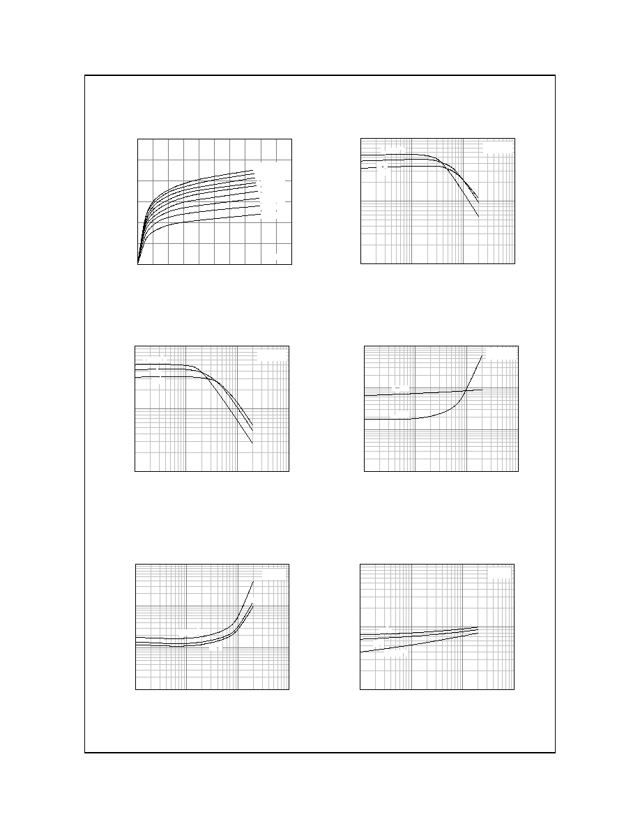
Figure 7. Switching Time
Figure 8. Forwrd Diode Voltage
Figure 9. Reverse Recovery Time
Figure 10. Collector Outpt Capacitance
Figure 11. Safe Operating Area
Figure 12. Power Derating
0.1
1
10
0.01
0.1
1
10
V
CC
= 300V
I
C
= 5I
B1
= -2.5I
B2
t
F
t
STG
t
ST
G
, t
F
[
µ
s],
T
I
M
E
I
C
[A], COLLECTOR CURRENT
0.01
0.1
1
10
0.1
1
10
V
f
[
V
]
,
F
O
RWA
RD DI
O
D
E
V
O
L
T
A
G
E
I
F
[A], FORWARD DIODE CURRENT
0.2
0.4
0.6
0.8
1.0
0.8
1.0
1.2
1.4
1.6
di/dt = 10A/
µ
s
tr
r
[
µ
s
]
,
RE
V
E
R
S
E
RE
CO
VE
RY
T
I
M
E
I
f
[A], FORWARD CURRENT
1
10
100
1
10
100
1000
f = 1MHz
C
ob
[p
F
], CA
P
A
C
IT
A
N
CE
V
CB
[V], COLLECTOR-BASE VOLTAGE
10
100
1000
0.01
0.1
1
10
100
10
µ
s
DC
1
µ
s
5ms
1ms
I
C
[
A
]
,
CO
LL
E
C
T
O
R CUR
RE
NT
V
CE
[V], COLLECTOR-EMITTER VOLTAGE
0
25
50
75
100
125
150
175
0
20
40
60
80
P
C
[W
], P
O
W
E
R
DIS
S
IP
A
T
IO
N
T
C
[
o
C], CASE TEMPERATURE

Package Dimensions
©2002 Fairchild Semiconductor Corporation
Rev. B1, December 2002
KSC530
2D
Dimensions in Millimeters
4.50
±
0.20
9.90
±
0.20
1.52
±
0.10
0.80
±
0.10
2.40
±
0.20
10.00
±
0.20
1.27
±
0.10
¯3.60
±
0.10
(8.70)
2.80
±
0.10
15.90
±
0.20
10.08
±
0.30
18.95MAX.
(1.70)
(3.70)
(3.00)
(1.46)
(1.00)
(45
∞
)
9.20
±
0.20
13.08
±
0.20
1.30
±
0.10
1.30
+0.10
≠0.05
0.50
+0.10
≠0.05
2.54TYP
[2.54
±
0.20
]
2.54TYP
[2.54
±
0.20
]
TO-220

©2002 Fairchild Semiconductor Corporation
Rev. I1
TRADEMARKS
The following are registered and unregistered trademarks Fairchild Semiconductor owns or is authorized to use and is
not intended to be an exhaustive list of all such trademarks.
DISCLAIMER
FAIRCHILD SEMICONDUCTOR RESERVES THE RIGHT TO MAKE CHANGES WITHOUT FURTHER NOTICE TO ANY
PRODUCTS HEREIN TO IMPROVE RELIABILITY, FUNCTION OR DESIGN. FAIRCHILD DOES NOT ASSUME ANY
LIABILITY ARISING OUT OF THE APPLICATION OR USE OF ANY PRODUCT OR CIRCUIT DESCRIBED HEREIN;
NEITHER DOES IT CONVEY ANY LICENSE UNDER ITS PATENT RIGHTS, NOR THE RIGHTS OF OTHERS.
LIFE SUPPORT POLICY
FAIRCHILD'S PRODUCTS ARE NOT AUTHORIZED FOR USE AS CRITICAL COMPONENTS IN LIFE SUPPORT
DEVICES OR SYSTEMS WITHOUT THE EXPRESS WRITTEN APPROVAL OF FAIRCHILD SEMICONDUCTOR
INTERNATIONAL.
As used herein:
1. Life support devices or systems are devices or systems
which, (a) are intended for surgical implant into the body,
or (b) support or sustain life, or (c) whose failure to perform
when properly used in accordance with instructions for use
provided in the labeling, can be reasonably expected to
result in significant injury to the user.
2. A critical component is any component of a life support
device or system whose failure to perform can be
reasonably expected to cause the failure of the life support
device or system, or to affect its safety or effectiveness.
PRODUCT STATUS DEFINITIONS
Definition of Terms
Datasheet Identification
Product Status
Definition
Advance Information
Formative or In
Design
This datasheet contains the design specifications for
product development. Specifications may change in
any manner without notice.
Preliminary
First Production
This datasheet contains preliminary data, and
supplementary data will be published at a later date.
Fairchild Semiconductor reserves the right to make
changes at any time without notice in order to improve
design.
No Identification Needed
Full Production
This datasheet contains final specifications. Fairchild
Semiconductor reserves the right to make changes at
any time without notice in order to improve design.
Obsolete
Not In Production
This datasheet contains specifications on a product
that has been discontinued by Fairchild semiconductor.
The datasheet is printed for reference information only.
FACTTM
FACT Quiet seriesTM
FAST
Æ
FASTrTM
FRFETTM
GlobalOptoisolatorTM
GTOTM
HiSeCTM
I
2
CTM
ImpliedDisconnectTM
ISOPLANARTM
LittleFETTM
MicroFETTM
MicroPakTM
MICROWIRETM
MSXTM
MSXProTM
OCXTM
OCXProTM
OPTOLOGIC
Æ
OPTOPLANARTM
PACMANTM
POPTM
Power247TM
PowerTrench
Æ
QFETTM
QSTM
QT OptoelectronicsTM
Quiet SeriesTM
RapidConfigureTM
RapidConnectTM
SILENT SWITCHER
Æ
SMART STARTTM
SPMTM
StealthTM
SuperSOTTM-3
SuperSOTTM-6
SuperSOTTM-8
SyncFETTM
TinyLogicTM
TruTranslationTM
UHCTM
UltraFET
Æ
VCXTM
ACExTM
ActiveArrayTM
BottomlessTM
CoolFETTM
CROSSVOLTTM
DOMETM
EcoSPARKTM
E
2
CMOSTM
EnSignaTM
Across the board. Around the world.TM
The Power FranchiseTM
Programmable Active DroopTM