 | –≠–ª–µ–∫—Ç—Ä–æ–Ω–Ω—ã–π –∫–æ–º–ø–æ–Ω–µ–Ω—Ç: MC4558CD | –°–∫–∞—á–∞—Ç—å:  PDF PDF  ZIP ZIP |
©2001 Fairchild Semiconductor Corporation
www.fairchildsemi.com
Rev. 1.0.1
Features
∑ No frequency compensation required.
∑ No latch up.
∑ Large common mode and differential voltage range.
∑ Parameter tracking over temperature range.
∑ Gain and phase match between amplifiers.
∑ Internally frequency compensated.
∑ Low noise input transistors.
Descriptions
The MC4558 series is a monolithic integrated circuit
designed for dual operational amplifier.
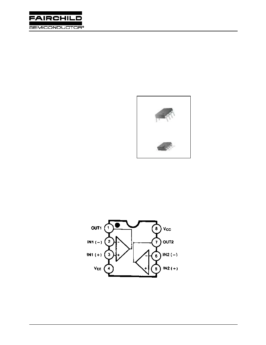
8-DIP
8-SOP
1
1
Internal Block Diagram
MC4558
Dual Operational Amplifier
MC4558
2
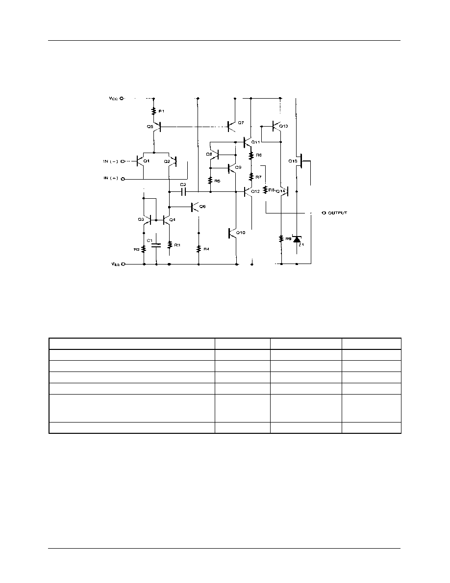
Schematic Diagram
(One Section Only)
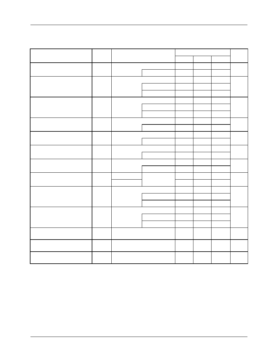
Absolute Maximum Ratings
Parameter
Symbol
Value
Unit
Supply Voltage
V
CC
±
22
V
Differential Input Voltage
V
I(DIFF)
30
V
Input Voltage
V
I
±
15
V
Power Dissipation
P
D
400
mW
Operating Temperature Range
MC4558C
MC4558V
T
OPR
0 ~ 70
-40 ~ 85
∞
C
Storage Temperature Range
T
STG
-65 ~ 150
∞
C
MC4558
3
Electrical Characteristics
(V
CC
= 15V, V
EE
= - 15V ,T
A
= 25
∞
C unless otherwise specified)
Note :
1. MC4558C : T
A(MIN)
T
A
T
A(MAX)
= 0
T
A
70
∞
C , MC4558V : T
A(MIN)
T
A
T
A(MAX)
= -40
T
A
+85
∞
C
2. Guaranteed by design.
Parameter Symbol
Conditions
MC4558C/MC4558V
Unit
Min
Typ
Max
Input Offset Voltage
V
IO
R
S
10K
-
2
6
mV
Note 1
-
-
7.5
Input Offset Current
I
IO
-
5
200
nA
T
A
=T
A(MAX)
-
-
300
T
A
=T
A(MIN)
-
-
300
Input Bias Current
I
BIAS
-
30
500
nA
T
A
=T
A(MAX)
-
-
800
T
A
=T
A(MIN)
-
-
800
Large Signal
Voltage Gain
G
V
V
O(P-P)
=
±
10V,R
L
2K
20
200
-
V/mV
Note 1
-
-
-
Common Mode Input
Voltage Range
V
I(R)
±
12
±
13
-
V
Note 1
-
-
-
Common Mode
Rejection Ratio
CMRR
R
S
10K
70
90
-
dB
Note 1
-
-
-
Supply Voltage
Rejection Ratio
PSRR
R
S
10K
76
90
-
dB
Note 1
76
90
-
Output Voltage Swing
V
O(P.P)
R
L
10K
±
12
±
14
-
V
R
L
2K
±
10
±
13
-
Supply Current
(Both Amplifiers)
I
CC
-
3.5
5.8
mA
T
A
=T
A(MAX)
-
-
5.0
T
A
=T
A(MIN)
-
-
6.7
Power Consumption
(Both Amplifiers)
P
C
-
70
170
mW
T
A
=T
A(MAX)
-
-
150
T
a
= T
A(MIN)
-
-
200
Slew Rate (Note2)
SR
V
I
=10V, R
L
2K
C
I
100pF
1.2
-
-
V/
µ
s
Rise Time (Note2)
T
R
V
I
=20mV, R
L
2K
C
I
100pF
-
0.3
-
µ
s
Overshoot (Note2)
OS
V
I
=20mV, R
L
2K
C
I
100pF
-
15
-
%
MC4558
4
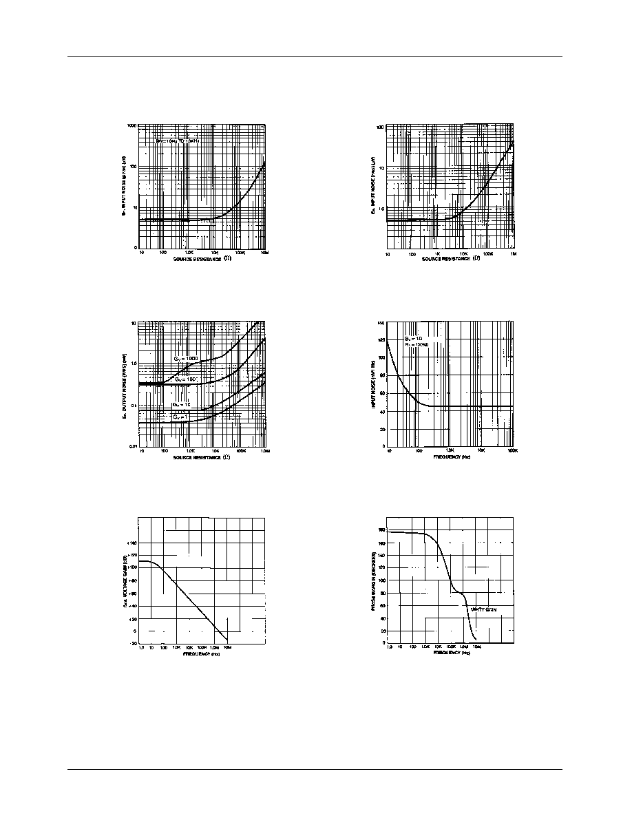
Typical Performance Characteristics
Figure 1. Burst Noise vs Source Resistance
Figure 2. RMS Noise vs Source Resistance
Figure 3. Output Noise vs Source Resistance
Figure 4. Spectral Noise Density
Figure 5. Open Loop Frequency Response
Figure 6. Phase Margin vs Frequency

MC4558
5
Typical Performance Characteristics (continued)
Figure 7. Positive Output Voltage Swing vs
Load Resistance
Figure 8. Negative Output Voltage Swing vs
Load Resistance
Figure 9. Power Bandwidth
(Large Signal Output Swing vs Frequency)