
September 1983
Revised February 1999
MM74HC157 Q
u
ad
2-
Inp
u
t M
u
l
t
i
p
l
exer
© 1999 Fairchild Semiconductor Corporation
DS005314.prf
www.fairchildsemi.com
MM74HC157
Quad 2-Input Multiplexer
General Description
The MM74HC157 high speed Quad 2-to-1 Line data selec-
tor/Multiplexers utilizes advanced silicon-gate CMOS tech-
nology. It possesses the high noise immunity and low
power consumption of standard CMOS integrated circuits,
as well as the ability to drive 10 LS-TTL loads.
This device consists of four 2-input digital multiplexers with
common select and STROBE inputs. When the STROBE
input is at logical "0" the four outputs assume the values as
selected from the inputs. When the STROBE input is at a
logical "1" the outputs assume logical "0".
The 74HC logic family is functionally as well as pin-out
compatible with the standard 74LS logic family. All inputs
are protected from damage due to static discharge by inter-
nal diode clamps to V
CC
and ground.
Features
s
Typical propagation delay: 14 ns data to any output
s
Wide power supply range: 2≠6V
s
Low power supply quiescent current: 80
µ
A maximum
(74HC Series)
s
Fan-out of 10 LS-TTL loads
s
Low input current: 1
µ
A maximum
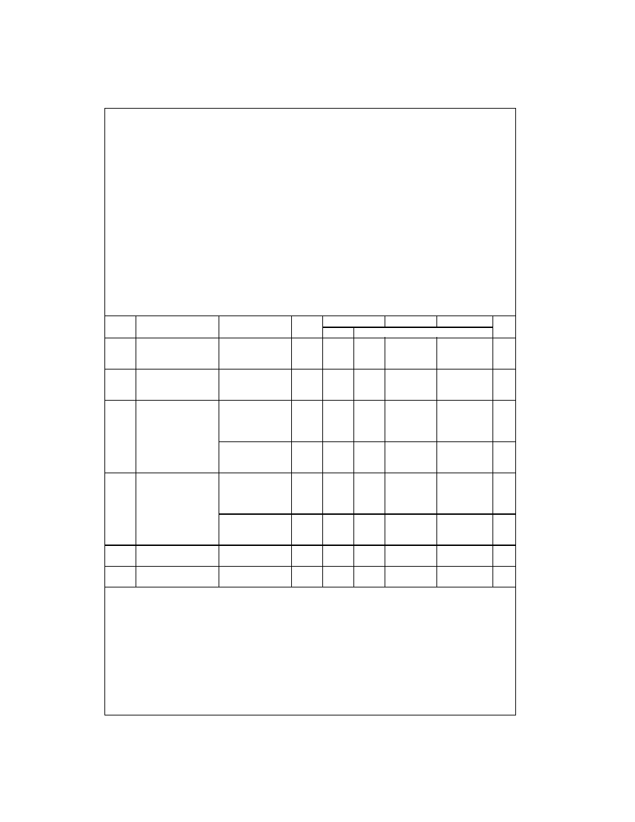
Ordering Code:
Devices also available in Tape and Reel. Specify by appending the suffix letter "X" to the ordering code.
Connection Diagram
Pin Assignments for DIP, SOIC, SOP and TSSOP
Top View
Function Table
H
=
HIGH Level,
L
=
LOW Level
X
=
Irrelevant
Order Number
Package Number
Package Description
MM74HC157M
M16A
16-Lead Small Outline Integrated Circuit (SOIC), JEDEC MS-012, 0.150" Narrow
MM74HC157SJ
M16D
16-Lead Small Outline Package (SOP), EIAJ TYPE II, 5.3mm Wide
MM74HC157MTC
MTC16
16-Lead Thin Shrink Small Outline Package (TSSOP), JEDEC MO-153, 4.4mm Wide
MM74HC157N
N16E
16-Lead Plastic Dual-In-Line Package (PDIP), JEDEC MS-001, 0.300" Wide
Inputs
Output
Strobe
Select
A
B
Y
H
X
X
X
L
L
L
L
X
L
L
L
H
X
H
L
H
X
L
L
L
H
X
H
H

www.fairchildsemi.com
2
MM
74HC157
Logic Diagram
3
www.fairchildsemi.com
MM74HC157
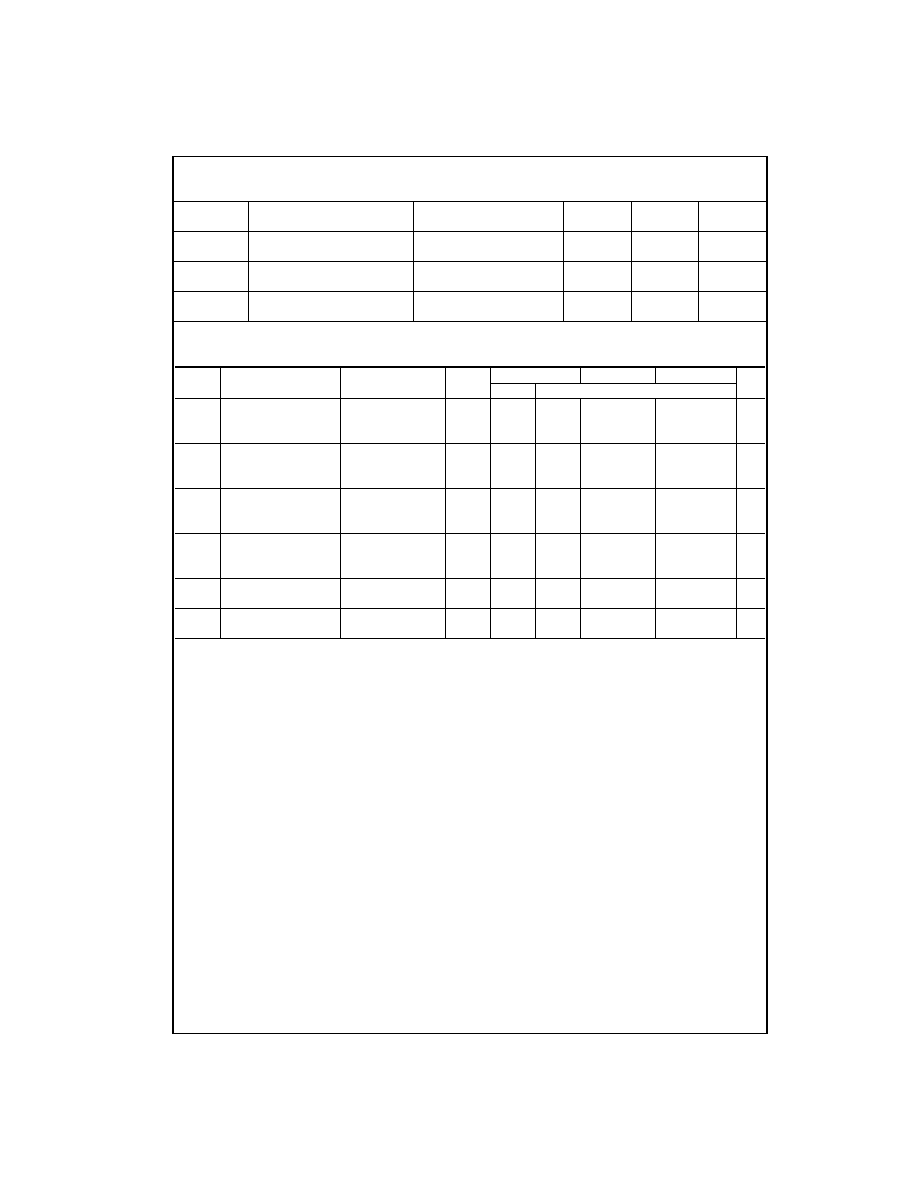
Absolute Maximum Ratings
(Note 1)
(Note 2)
Recommended Operating
Conditions
Note 1: Absolute Maximum Ratings are those values beyond which dam-
age to the device may occur.
Note 2: Unless otherwise specified all voltages are referenced to ground.
Note 3: Power Dissipation temperature derating -- plastic "N" package:
-
12 mW/
∞
C from 65
∞
C to 85
∞
C.
DC Electrical Characteristics
(Note 4)
Note 4: For a power supply of 5V
±
10% the worst case output voltages (V
OH
, and V
OL
) occur for HC at 4.5V. Thus the 4.5V values should be used when
designing with this supply. Worst case V
IH
and V
IL
occur at V
CC
=
5.5V and 4.5V respectively. (The V
IH
value at 5.5V is 3.85V.) The worst case leakage cur-
rent (I
IN
, I
CC
, and I
OZ
) occur for CMOS at the higher voltage and so the 6.0V values should be used.
Supply Voltage (V
CC
)
-
0.5 to
+
7.0V
DC Input Voltage (V
IN
)
-
1.5 to V
CC
+
1.5V
DC Output Voltage (V
OUT
)
-
0.5 to V
CC
+
0.5V
Clamp Diode Current (I
IK
, I
OK
)
±
20 mA
DC Output Current, per pin (I
OUT
)
±
25 mA
DC V
CC
or GND Current, per pin (I
CC
)
±
50 mA
Storage Temperature Range (T
STG
)
-
65
∞
C to
+
150
∞
C
Power Dissipation (P
D
)
(Note 3)
600 mW
S.O. Package only
500 mW
Lead Temperature (T
L
)
(Soldering 10 seconds)
260
∞
C
Min
Max
Units
Supply Voltage (V
CC
)
2
6
V
DC Input or Output Voltage
0
V
CC
V
(V
IN
, V
OUT
)
Operating Temperature Range (T
A
)
-
40
+
85
∞
C
Input Rise or Fall Times
(t
r
, t
f
) V
CC
=
2.0V
1000
ns
V
CC
=
4.5V
500
ns
V
CC
=
6.0V
400
ns
Symbol
Parameter
Conditions
V
CC
T
A
=
25
∞
C
T
A
=
-
40 to 85
∞
C T
A
=
-
55 to 125
∞
C
Units
Typ
Guaranteed Limits
V
IH
Minimum HIGH Level
2.0V
1.5
1.5
1.5
V
Input Voltage
4.5V
3.15
3.15
3.15
V
6.0V
4.2
4.2
4.2
V
V
IL
Maximum LOW Level
2.0V
0.5
0.5
0.5
V
Input Voltage
4.5V
1.35
1.35
1.35
V
6.0V
1.8
1.8
1.8
V
V
OH
Minimum HIGH Level
V
IN
=
V
IH
or V
IL
Output Voltage
|I
OUT
|
20
µ
A
2.0V
2.0
1.9
1.9
1.9
V
4.5V
4.5
4.4
4.4
4.4
V
6.0V
6.0
5.9
5.9
5.9
V
V
IN
=
V
IH
or V
IL
|I
OUT
|
4.0 mA
4.5V
4.2
3.98
3.84
3.7
V
|I
OUT
|
5.2 mA
6.0V
5.7
5.48
5.34
5.2
V
V
OL
Maximum LOW Level
V
IN
=
V
IH
or V
IL
Output Voltage
|I
OUT
|
20
µ
A
2.0V
0
0.1
0.1
0.1
V
4.5V
0
0.1
0.1
0.1
V
6.0V
0
0.1
0.1
0.1
V
V
IN
=
V
IH
or V
IL
|I
OUT
|
4.0 mA
4.5V
0.2
0.26
0.33
0.4
V
|I
OUT
|
5.2 mA
6.0V
0.2
0.26
0.33
0.4
V
I
IN
Maximum Input
V
IN
=
V
CC
or GND
6.0V
±
0.1
±
1.0
±
1.0
µ
A
Current
I
CC
Maximum Quiescent
V
IN
=
V
CC
or GND
6.0V
8.0
80
160
µ
A
Supply Current
I
OUT
=
0
µ
A
www.fairchildsemi.com
4
MM
74HC157
AC Electrical Characteristics
V
CC
=
5V, T
A
=
25
∞
C, C
L
=
15 pF, t
r
=
t
f
=
6 ns
AC Electrical Characteristics
C
L
=
50 pF, t
r
=
t
f
=
6 ns (unless otherwise specified)
Note 5: C
PD
determines the no load dynamic power consumption, P
D
=
C
PD
V
CC
2
f
+
I
CC
V
CC
, and the no load dynamic current consumption,
I
S
=
C
PD
V
CC
f
+
I
CC
.
Symbol
Parameter
Conditions
Typ
Guaranteed
Units
Limit
t
PHL
, t
PLH
Maximum Propagation
14
20
ns
Delay, Data to Output
t
PHL
, t
PLH
Maximum Propagation
14
20
ns
Delay, Select to Output
t
PHL
, t
PLH
Maximum Propagation
12
18
ns
Delay, Strobe to Output
Symbol
Parameter
Conditions
V
CC
T
A
=
25
∞
C
T
A
=
-
40 to 85
∞
C T
A
=
-
55 to 125
∞
C
Units
Typ
Guaranteed Limits
t
PHL
, t
PLH
Maximum Propagation
2.0V
63
125
158
186
ns
Delay, Data to Output
4.5V
13
25
32
37
ns
6.0V
11
21
27
32
ns
t
PHL
, t
PLH
Maximum Propagation
2.0V
63
125
158
186
ns
Delay, Select to Output
4.5V
13
25
32
37
ns
6.0V
11
21
27
32
ns
t
PHL
, t
PLH
Maximum Propagation
2.0V
58
115
145
171
ns
Delay, Strobe to Output
4.5V
12
23
29
34
ns
6.0V
10
20
25
29
ns
t
TLH
, t
THL
Maximum Output Rise
2.0V
30
75
95
110
ns
and Fall Time
4.5V
8
15
19
22
ns
6.0V
7
13
16
19
ns
C
IN
Maximum Input
5
10
10
10
pF
Capacitance
C
PD
Power Dissipation
(per
57
pF
Capacitance (Note 5)
Multiplexer)
5
www.fairchildsemi.com
MM74HC157
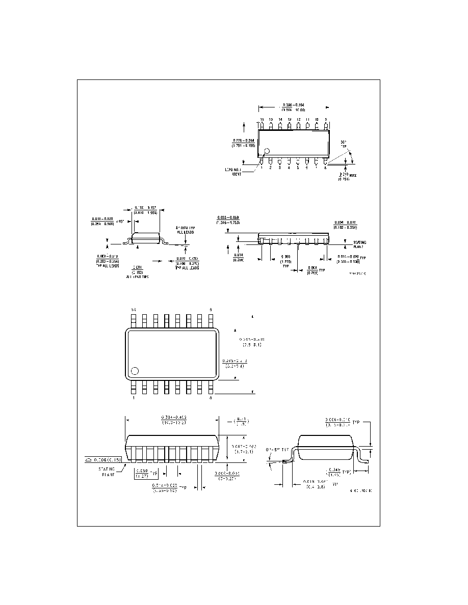
Physical Dimensions
inches (millimeters) unless otherwise noted
16-Lead Small Outline Integrated Circuit (SOIC), JEDEC MS-012, 0.150" Narrow
Package Number M16A
16-Lead Small Outline Package (SOP), EIAJ TYPE II, 5.3mm Wide
Package Number M16D