September 1983
Revised February 1999
MM74HC161
∑ MM74HC163 Sy
nchronous
Bin
a
ry
Counter
wi
th
Asynchrono
us Cl
ear
∑ Synch
ronous
Binar
y
Coun
ter wit
h
Sy
nchronous Cle
a
r
© 1999 Fairchild Semiconductor Corporation
DS005008.prf
www.fairchildsemi.com
MM74HC161 ∑ MM74HC163
Synchronous Binary Counter with Asynchronous Clear
∑ Synchronous Binary Counter with Synchronous Clear
General Description
The MM74HC161 and MM74HC163 synchronous presetta-
ble counters utilize advanced silicon-gate CMOS technol-
ogy and internal look-ahead carry logic for use in high
speed counting applications. They offer the high noise
immunity and low power consumption inherent to CMOS
with speeds similar to low power Schottky TTL. The HC161
and the HC163 are 4 bit binary counters. All flip-flops are
clocked simultaneously on the LOW-to-HIGH transition
(positive edge) of the CLOCK input waveform.
These counters may be preset using the LOAD input. Pre-
setting of all four flip-flops is synchronous to the rising edge
of CLOCK. When LOAD is held LOW counting is disabled
and the data on the A, B, C, and D inputs is loaded into the
counter on the rising edge of CLOCK. If the load input is
taken HIGH before the positive edge of CLOCK the count
operation will be unaffected.
All of these counters may be cleared by utilizing the
CLEAR input. The clear function on the MM74HC163
counter is synchronous to the clock. That is, the counters
are cleared on the positive edge of CLOCK while the clear
input is held LOW.
The MM74HC161 counter is cleared asynchronously.
When the CLEAR is taken LOW the counter is cleared
immediately regardless of the CLOCK.
Two active HIGH enable inputs (ENP and ENT) and a RIP-
PLE CARRY (RC) output are provided to enable easy cas-
cading of counters. Both ENABLE inputs must be HIGH to
count. The ENT input also enables the RC output. When
enabled, the RC outputs a positive pulse when the counter
overflows. This pulse is approximately equal in duration to
the HIGH level portion of the Q
A
output. The RC output is
fed to successive cascaded stages to facilitate easy imple-
mentation of N-bit counters.
All inputs are protected from damage due to static dis-
charge by diodes to V
CC
and ground.
Features
s
Typical operating frequency: 40 MHz
s
Typical propagation delay; clock to Q: 18 ns
s
Low quiescent current: 80
µ
A maximum (74HC Series)
s
Low input current: 1
µ
A maximum
s
Wide power supply range: 2≠6V
Ordering Code:
Devices also available in Tape and Reel. Specify by appending the suffix letter "X" to the ordering code.
Order Number
Package Number
Package Description
MM74HC161M
M16A
16-Lead Small Outline Integrated Circuit (SOIC), JEDEC MS-012, 0.150" Narrow
MM74HC161SJ
M16D
16-Lead Small Outline Package (SOP), EIAJ TYPE II, 5.3mm Wide
MM74HC161MTC
MTC16
16-Lead Thin Shrink Small Outline Package (TSSOP), JEDEC MO-153, 4.4mm Wide
MM74HC161N
N16E
16-Lead Plastic Dual-In-Line Package (PDIP), JEDEC MS-001, 0.300" Wide
MM74HC163M
M16A
16-Lead Small Outline Integrated Circuit (SOIC), JEDEC MS-012, 0.150" Narrow
MM74HC163SJ
M16D
16-Lead Small Outline Package (SOP), EIAJ TYPE II, 5.3mm Wide
MM74HC163MTC
MTC16
16-Lead Thin Shrink Small Outline Package (TSSOP), JEDEC MO-153, 4.4mm Wide
MM74HC163N
N16E
16-Lead Plastic Dual-In-Line Package (PDIP), JEDEC MS-001, 0.300" Wide
www.fairchildsemi.com
2
MM74HC161
∑ MM
74HC163
Connection Diagram
Pin Assignments for DIP, SOIC, SOP and TSSOP
Truth Tables
MM74HC161
MM74HC163
H
=
HIGH Level
L
=
LOW Level
X
=
Don't Care
=
LOW-to-HIGH Transition
Logic Diagram
CLK
CLR
ENP
ENT
Load
Function
X
L
X
X
X
Clear
X
H
H
L
H
Count & RC disabled
X
H
L
H
H
Count disabled
X
H
L
L
H
Count & RC disabled
H
X
X
L
Load
H
H
H
H
Increment Counter
CLK
CLR
ENP
ENT
Load
Function
L
X
X
X
Clear
X
H
H
L
H
Count & RC disabled
X
H
L
H
H
Count disabled
X
H
L
L
H
Count & RC disabled
H
X
X
L
Load
H
H
H
H
Increment Counter
3
www.fairchildsemi.com
MM74HC161
∑ MM74HC163
Absolute Maximum Ratings
(Note 1)
(Note 2)
Recommended Operating
Conditions
Note 1: Absolute Maximum Ratings are those values beyond which dam-
age to the device may occur.
Note 2: Unless otherwise specified all voltages are referenced to ground.
Note 3: Power Dissipation temperature derating -- plastic "N" package:
-
12 mW/
∞
C from 65
∞
C to 85
∞
C.
DC Electrical Characteristics
(Note 4)
Note 4: For a power supply of 5V
±
10% the worst case output voltages (V
OH
, and V
OL
) occur for HC at 4.5V. Thus the 4.5V values should be used when
designing with this supply. Worst case V
IH
and V
IL
occur at V
CC
=
5.5V and 4.5V respectively. (The V
IH
value at 5.5V is 3.85V.) The worst case leakage current
(I
IN
, I
CC
, and I
OZ
) occur for CMOS at the higher voltage and so the 6.0V values should be used.
Supply Voltage (V
CC
)
-
0.5 to
+
7.0V
DC Input Voltage (V
IN
)
-
1.5 to V
CC
+
1.5V
DC Output Voltage (V
OUT
)
-
0.5 to V
CC
+
0.5V
Clamp Diode Current (I
IK
, I
OK
)
±
20 mA
DC Output Current, per pin
(I
OUT
)
±
25 mA
DC V
CC
or GND Current, per pin
(I
CC
)
±
50 mA
Storage Temperature Range (T
STG
)
-
65
∞
C to
+
150
∞
C
Power Dissipation (P
D
)
(Note 3)
600 mW
S.O. Package only
500 mW
Lead Temperature
(T
L
) (Soldering 10 seconds)
260
∞
C
Min
Max
Units
Supply Voltage (V
CC
)
2
6
V
DC Input or Output Voltage
0
V
CC
V
(V
IN
, V
OUT
)
Operating Temperature Range (T
A
)
-
40
+
85
∞
C
Input Rise or Fall Times
(t
r
, t
f
) V
CC
=
2.0V
1000
ns
V
CC
=
4.5V
500
ns
V
CC
=
6.0V
400
ns
Symbol
Parameter
Conditions
V
CC
T
A
=
25
∞
C
T
A
=-
40 to 85
∞
C T
A
=-
55 to 125
∞
C
Units
Typ
Guaranteed Limits
V
IH
Minimum HIGH Level
2.0V
1.5
1.5
1.5
V
Input Voltage
4.5V
3.15
3.15
3.15
V
6.0V
4.2
4.2
4.2
V
V
IL
Maximum LOW Level
2.0V
0.5
0.5
0.5
V
Input Voltage
4.5V
1.35
1.35
1.35
V
6.0V
1.8
1.8
1.8
V
V
OH
Minimum HIGH Level
V
IN
=
V
IH
or V
IL
Output Voltage
|I
OUT
|
20
µ
A
2.0V
2.0
1.9
1.9
1.9
V
4.5V
4.5
4.4
4.4
4.4
V
6.0V
6.0
5.9
5.9
5.9
V
V
IN
=
V
IH
or V
IL
|I
OUT
|
4.0 mA
4.5V
4.2
3.98
3.84
3.7
V
|I
OUT
|
5.2 mA
6.0V
5.7
5.48
5.34
5.2
V
V
OL
Maximum LOW Level
V
IN
=
V
IH
or V
IL
Output Voltage
|I
OUT
|
20
µ
A
2.0V
0
0.1
0.1
0.1
V
4.5V
0
0.1
0.1
0.1
V
6.0V
0
0.1
0.1
0.1
V
V
IN
=
V
IH
or V
IL
|I
OUT
|
4.0 mA
4.5V
0.2
0.26
0.33
0.4
V
|I
OUT
|
5.2 mA
6.0V
0.2
0.26
0.33
0.4
V
I
IN
Maximum Input
V
IN
=
V
CC
or GND
6.0V
±
0.1
±
1.0
±
1.0
µ
A
Current
I
CC
Maximum Quiescent
V
IN
=
V
CC
or GND
6.0V
8.0
80
160
µ
A
Supply Current
I
OUT
=
0
µ
A
www.fairchildsemi.com
4
MM74HC161
∑ MM
74HC163
AC Electrical Characteristics
V
CC
=
5V, T
A
=
25
∞
C, C
L
=
15 pF, t
r
=
t
f
=
6 ns
AC Electrical Characteristics
C
L
=
50 pF, t
r
=
t
f
=
6 ns
(unless otherwise specified)
Symbol
Parameter
Conditions
Typ
Guaranteed Limit
Units
f
MAX
Maximum Operating Frequency
43
30
MHz
t
PHL
, t
PLH
Maximum Propagation Delay, Clock to RC
30
35
ns
t
PHL
, t
PLH
Maximum Propagation Delay, Clock to Q
29
34
ns
t
PHL
, t
PLH
Maximum Propagation Delay, ENT to RC
18
32
ns
t
PHL
Maximum Propagation Delay, Clear to Q or RC
27
38
ns
t
REM
Minimum Removal Time, Clear to Clock
10
20
ns
t
S
Minimum Set Up Time Clear, Load,
30
ns
Enable or Data to Clock
t
H
Minimum Hold Time, Data from Clock
5
ns
t
W
Minimum Pulse Width Clock,
16
ns
Clear, or Load
Symbol
Parameter
Conditions
V
CC
T
A
=
25
∞
C
T
A
=-
40 to 85
∞
C T
A
=-
55 to 125
∞
C
Units
Typ
Guaranteed Limits
f
MAX
Maximum Operating
2.0V
10
5
4
4
MHz
Frequency
4.5V
40
27
21
18
MHz
6.0V
45
32
25
21
MHz
t
PHL
Maximum Propagation
2.0V
100
215
271
320
ns
Delay, Clock to RC
4.5V
32
43
54
64
ns
6.0V
28
37
46
54
ns
t
PLH
Maximum Propagation
2.0V
88
175
220
260
ns
Delay, Clock to RC
4.5V
18
35
44
52
ns
6.0V
15
30
37
44
ns
t
PHL
Maximum Propagation
2.0V
95
205
258
305
ns
Delay, Clock to Q
4.5V
30
41
52
61
ns
6.0V
26
35
44
52
ns
t
PLH
Maximum Propagation
2.0V
85
170
214
253
ns
Delay, Clock to Q
4.5V
17
34
43
51
ns
6.0V
14
29
36
43
ns
t
PHL
Maximum Propagation
2.0V
90
195
246
291
ns
Delay, ENT to RC
4.5V
28
39
49
58
ns
6.0V
24
33
42
49
ns
t
PLH
Maximum Propagation
2.0V
80
160
202
238
ns
Delay, ENT to RC
4.5V
16
32
40
48
ns
6.0V
14
27
34
41
ns
t
PHL
Maximum Propagation
2.0V
100
220
275
325
ns
Delay, Clear to RC
4.5V
32
44
55
66
ns
6.0V
28
37
47
55
ns
t
PHL
Maximum Propagation
2.0V
100
210
260
315
ns
Delay, Clear to Q
4.5V
32
42
52
63
ns
6.0V
28
36
45
54
ns
t
REM
Minimum Removal
2.0V
125
158
186
ns
Time Clear to Clock
4.5V
25
32
37
ns
6.0V
21
27
32
ns
t
S
Minimum Setup
2.0V
150
190
225
ns
Time Clear or Data
4.5V
30
38
45
ns
to Clock
6.0V
26
32
38
ns
t
S
Minimum Setup
2.0V
135
170
200
ns
Time Load
4.5V
27
34
41
ns
to Clock
6.0V
23
29
35
ns
5
www.fairchildsemi.com
MM74HC161
∑ MM74HC163
AC Electrical Characteristics
(Continued)
Note 5: C
PD
determines the no load dynamic power consumption, P
D
=
C
PD
V
CC
2
f
+
I
CC
V
CC
, and the no load dynamic current consumption,
I
S
=
C
PD
V
CC
f
+
I
CC
.
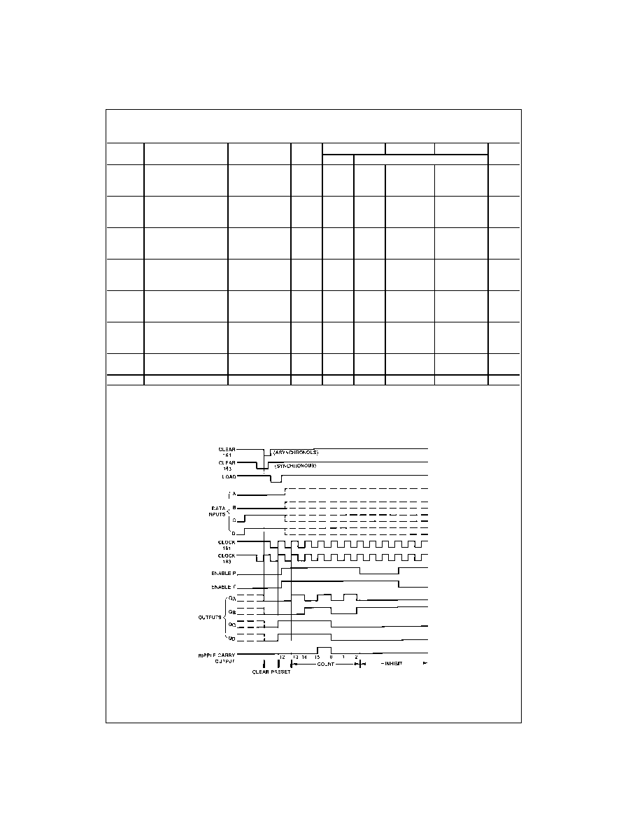
Logic Waveforms
Synchronous Binary Counters Typical Clear, Preset, Count and Inhibit Sequences
Sequence: (1) Clear outputs to zero (2) Preset to binary twelve (3) Count to thirteen, fourteen, fifteen, zero, one and two (4) Inhibit
Symbol
Parameter
Conditions
V
CC
T
A
=
25
∞
C
T
A
=-
40 to 85
∞
C T
A
=-
55 to 125
∞
C
Units
Typ
Guaranteed Limits
t
S
Minimum Setup
2.0V
175
220
260
ns
Time Enable
4.5V
35
44
52
ns
to Clock
6.0V
30
37
44
ns
t
H
Minimum Hold Time
2.0V
50
63
75
ns
Data from Clock
4.5V
10
13
15
ns
6.0V
9
11
13
ns
t
H
Minimum Hold Time
2.0V
0
0
0
ns
Enable, Load or Clear
4.5V
0
0
0
ns
to Clock
6.0V
0
0
0
ns
t
W
Minimum Pulse Width
2.0V
80
100
120
ns
Clock, Clear, or
4.5V
16
20
24
ns
Load
6.0V
14
17
20
ns
t
TLH
, t
THL
Maximum
2.0V
40
75
95
110
ns
Output Rise and
4.5V
8
15
19
22
ns
Fall Time
6.0V
7
13
16
19
ns
t
r
, t
f
Maximum Input Rise
2.0V
1000
1000
1000
ns
and Fall Time
4.5V
500
500
500
500
ns
6.0V
400
400
400
ns
C
PD
Powert Dissipation
(per package)
90
pF
Capacitance (Note 5)
C
IN
Maximum Input Capacitance
5
10
10
10
pF
www.fairchildsemi.com
6
MM74HC161
∑ MM
74HC163
Physical Dimensions
inches (millimeters) unless otherwise noted
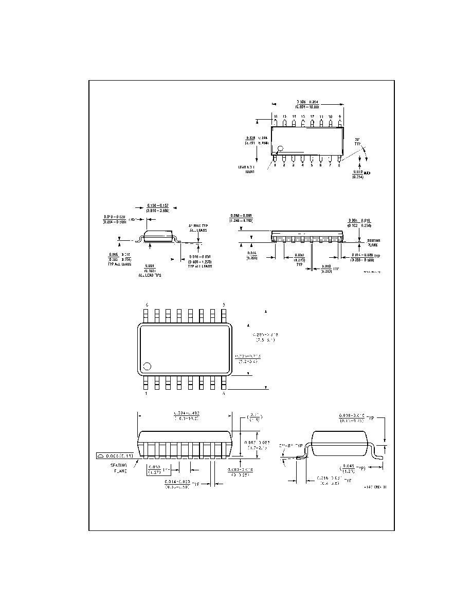
16-Lead Small Outline Integrated Circuit (SOIC), JEDEC MS-012, 0.150" Narrow
Package Number M16A
16-Lead Small Outline Package (SOP), EIAJ TYPE II, 5.3mm Wide
Package Number M16D

7
www.fairchildsemi.com
MM74HC161
∑ MM74HC163
Physical Dimensions
inches (millimeters) unless otherwise noted (Continued)
16-Lead Thin Shrink Small Outline Package (TSSOP), JEDEC MO-153, 4.4mm Wide
Package Number MTC16
Fairchild does not assume any responsibility for use of any circuitry described, no circuit patent licenses are implied and Fairchild reserves the right at any time without notice to change said circuitry and specifications.
MM74HC161
∑ MM
74
H
C
16
3
Synchr
onous Binar
y
Count
er wit
h
Asyn
chronous Clea
r
∑ Synchr
onous
Bi
nary
Count
er w
i
th
Synchr
onous C
l
ear
LIFE SUPPORT POLICY
FAIRCHILD'S PRODUCTS ARE NOT AUTHORIZED FOR USE AS CRITICAL COMPONENTS IN LIFE SUPPORT
DEVICES OR SYSTEMS WITHOUT THE EXPRESS WRITTEN APPROVAL OF THE PRESIDENT OF FAIRCHILD
SEMICONDUCTOR CORPORATION. As used herein:
1. Life support devices or systems are devices or systems
which, (a) are intended for surgical implant into the
body, or (b) support or sustain life, and (c) whose failure
to perform when properly used in accordance with
instructions for use provided in the labeling, can be rea-
sonably expected to result in a significant injury to the
user.
2. A critical component in any component of a life support
device or system whose failure to perform can be rea-
sonably expected to cause the failure of the life support
device or system, or to affect its safety or effectiveness.
www.fairchildsemi.com
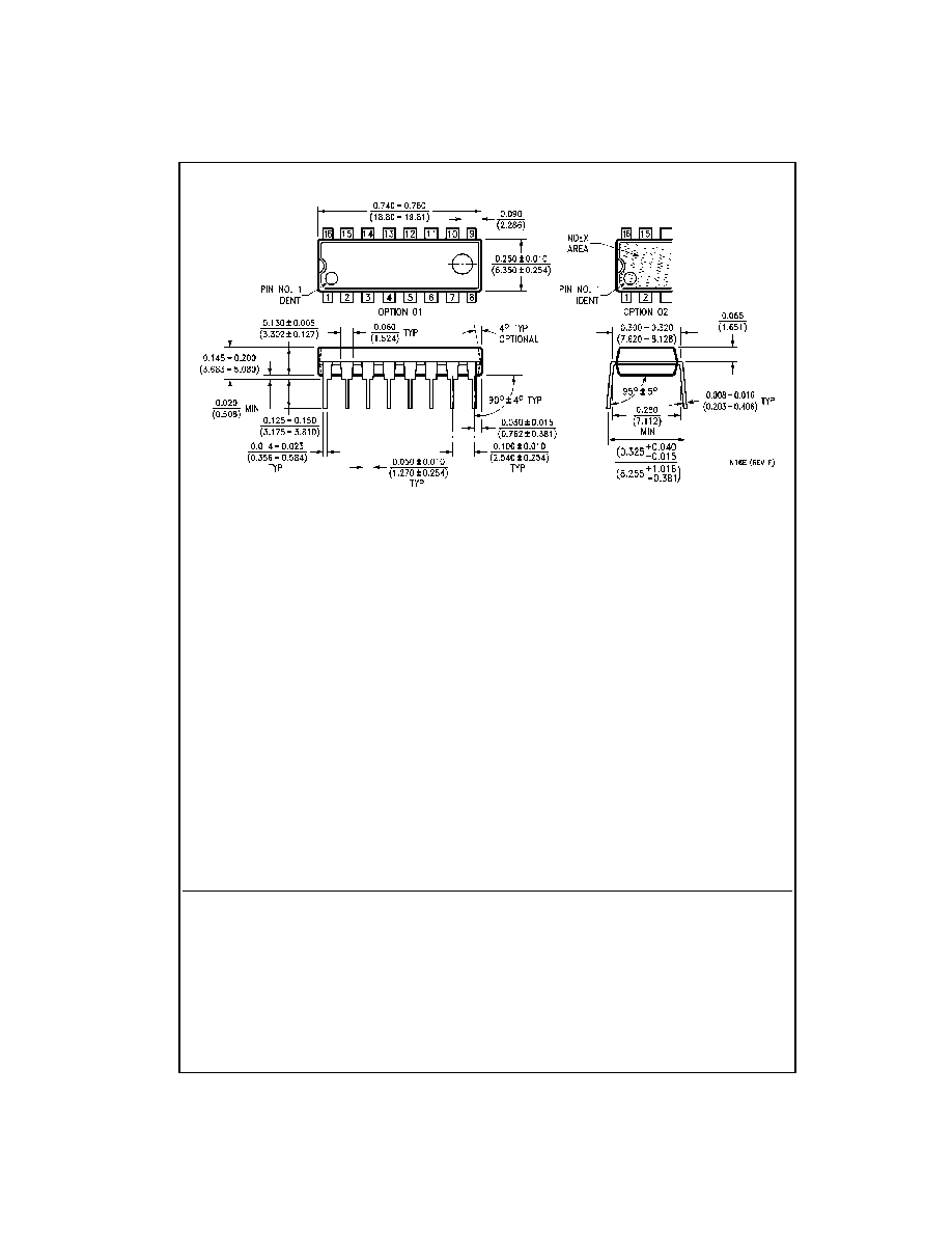
Physical Dimensions
inches (millimeters) unless otherwise noted (Continued)
16-Lead Plastic Dual-In-Line Package (PDIP), JEDEC MS-001, 0.300" Wide
Package Number N16E