
© 2000 Fairchild Semiconductor Corporation
DS005020
www.fairchildsemi.com
September 1983
Revised August 2000
MM74HC240 Inve
rti
ng O
c
t
a
l
3-
ST
A
T
E Buff
er
MM74HC240
Inverting Octal 3-STATE Buffer
General Description
The MM74HC240 3-STATE buffer utilizes advanced sili-
con-gate CMOS technology. It possesses high drive cur-
rent outputs which enable high speed operation even when
driving large bus capacitances. These circuits achieve
speeds comparable to low power Schottky devices, while
retaining the advantage of CMOS circuitry, i.e., high noise
immunity and low power consumption. It has a fanout of 15
LS-TTL equivalent inputs.
The MM74HC240 is an inverting buffer and has two active
LOW enables (1G and 2G). Each enable independently
controls 4 buffers.
All inputs are protected from damage due to static dis-
charge by diodes to V
CC
and ground.
Features
s
Typical propagation delay: 12 ns
s
3-STATE outputs for connection to system buses
s
Wide power supply range: 2≠6V
s
Low quiescent supply current: 80
µ
A (74 Series)
s
Output current: 6 mA
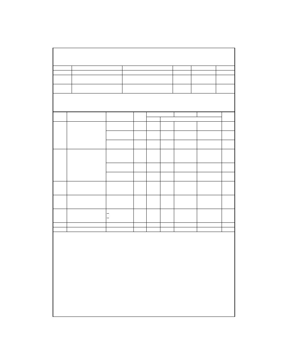
Ordering Code:
Devices also available in Tape and Reel. Specify by appending the suffix letter "X" to the ordering code.
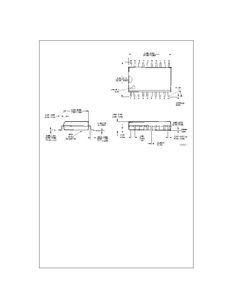
Connection Diagram
Top View
Truth Table
H
=
HIGH Level
L
=
LOW Level
Z
=
HIGH Impedance
Order Number
Package Number
Package Description
MM74HC240WM
M20B
20-Lead Small Outline Integrated Circuit (SOIC), JEDEC MS-013, 0.300 Wide
MM74HC240SJ
M20D
20-Lead Small Outline Package (SOP), EIAJ TYPE II, 5.3mm Wide
MM74HC240MTC
MTC20
20-Lead Thin Shrink Small Outline Package (TSSOP), JEDEC MO-153, 4.4mm Wide
MM74HC240N
N20A
20-Lead Plastic Dual-In-Line Package (PDIP), JEDEC MS-001, 0.300 Wide
1G
1A
1Y
2G
2A
2Y
L
L
H
L
L
H
L
H
L
L
H
L
H
L
Z
H
L
Z
H
H
Z
H
H
Z

www.fairchildsemi.com
2
MM
74HC240
Logic Diagram

3
www.fairchildsemi.com
MM74HC240
Absolute Maximum Ratings
(Note 1)
(Note 2)
Recommended Operating
Conditions
Note 1: Absolute Maximum Ratings are those values beyond which dam-
age to the device may occur.
Note 2: unless otherwise specified all voltages are referenced to ground.
Note 3: Power Dissipation temperature derating -- plastic "N" package:
-
12 mW/
∞
C from 65
∞
C to 85
∞
C.
DC Electrical Characteristics
(Note 4)
Note 4: For a power supply of 5V
±
10% the worst case output voltages (V
OH
, and V
OL
) occur for HC at 4.5V. Thus the 4.5V values should be used when
designing with this supply. Worst case V
IH
and V
IL
occur at V
CC
=
5.5V and 4.5V respectively. (The V
IH
value at 5.5V is 3.85V.) The worst case leakage cur-
rent (I
IN
, I
CC
, and I
OZ
) occur for CMOS at the higher voltage and so the 6.0V values should be used.
Supply Voltage (V
CC
)
-
0.5 to
+
7.0V
DC Input Voltage (V
IN
)
-
1.5 to V
CC
+
1.5V
DC Output Voltage (V
OUT
)
-
0.5 to V
CC
+
0.5V
Clamp Diode Current (I
IK
, I
OK
)
±
20 mA
DC Output Current, per pin (I
OUT
)
±
35 mA
DC V
CC
or GND Current, per pin (I
CC
)
±
70 mA
Storage Temperature Range (T
STG
)
-
65
∞
C to
+
150
∞
C
Power Dissipation (P
D
)
(Note 3)
600 mW
S.O. Package only
500 mW
Lead Temperature (T
L
)
(Soldering 10 seconds)
260
∞
C
Min
Max
Units
Supply Voltage (V
CC
)
2
6
V
DC Input or Output Voltage
0
V
CC
V
(V
IN
, V
OUT
)
Operating Temperature Range (T
A
)
-
40
+
85
∞
C
Input Rise or Fall Times
(t
r
, t
f
) V
CC
=
2.0V
1000
ns
V
CC
=
4.5V
500
ns
V
CC
=
6.0V
400
ns
Symbol
Parameter
Conditions
V
CC
T
A
=
25
∞
C
T
A
=
-
40 to 85
∞
C T
A
=
-
55 to 125
∞
C
Units
Typ
Guaranteed Limits
V
IH
Minimum HIGH Level
2.0V
1.5
1.5
1.5
V
Input Voltage
4.5V
3.15
3.15
3.15
V
6.0V
4.2
4.2
4.2
V
V
IL
Maximum LOW Level
2.0V
0.5
0.5
0.5
V
Input Voltage
4.5V
1.35
1.35
1.35
V
6.0V
1.8
1.8
1.8
V
V
OH
Minimum HIGH Level
V
I N
=
V
IH
or V
IL
Output Voltage
|I
OUT
|
20
µ
A
2.0V
2.0
1.9
1.9
1.9
V
4.5V
4.5
4.4
4.4
4.4
V
6.0V
6.0
5.9
5.9
5.9
V
V
IN
=
V
IH
or V
IL
|I
OUT
|
6.0 mA
4.5V
4.2
3.98
3.84
3.7
V
|I
OUT
|
7.8 mA
6.0V
5.7
5.48
5.34
5.2
V
V
OL
Maximum LOW Level
V
IN
=
V
IH
or V
IL
Output Voltage
|I
OUT
|
20
µ
A
2.0V
0
0.1
0.1
0.1
V
4.5V
0
0.1
0.1
0.1
V
6.0V
0
0.1
0.1
0.1
V
V
IN
=
V
IH
or V
IL
|I
OUT
|
6.0 mA
4.5V
0.2
0.26
0.33
0.4
V
|I
OUT
|
7.8 mA
6.0V
0.2
0.26
0.33
0.4
V
I
IN
Maximum Input Current
V
IN
=
V
CC
or GND
6.0V
±
0.1
±
1.0
±
1.0
µ
A
I
OZ
Maximum 3-STATE
V
IN
=
V
IH
or V
IL
Output Leakage
V
OUT
=
V
CC
or GND
6.0V
±
0.5
±
5
±
10
µ
A
Current
G
=
V
IH
, G
=
V
IL
I
CC
Maximum Quiescent
V
IN
=
V
CC
or GND
6.0V
8.0
80
160
µ
A
Supply Current
I
OUT
=
0
µ
A
www.fairchildsemi.com
4
MM
74HC240
AC Electrical Characteristics
V
CC
=
5V, T
A
=
25
∞
C, t
r
=
t
f
=
6 ns
AC Electrical Characteristics
V
CC
=
2.0V to 6.0V, C
L
=
50 pF, t
r
=
t
f
=
6 ns (unless otherwise specified)
Note 5: C
PD
determines the no load dynamic power consumption, P
D
=
C
PD
V
CC
2
f
+
I
CC
V
CC
, and the no load dynamic current consumption,
I
S
=
C
PD
V
CC
f
+
I
CC
.
Symbol
Parameter
Conditions
Typ
Guaranteed Limit
Units
t
PHL
, t
PLH
Maximum Propagation Delay
C
L
=
45 pF
12
18
ns
t
PZH
, t
PZL
Maximum Enable Delay
R
L
=
1 k
14
28
ns
to Active Output
C
L
=
45 pF
t
PHZ
, t
PLZ
Maximum Disable Delay
R
L
=
1 k
13
25
ns
from Active Output
C
L
=
5 pF
Symbol
Parameter
Conditions
V
CC
T
A
=
25
∞
C
T
A
=
-
40 to 85
∞
C T
A
=
-
55 to 125
∞
C
Units
Typ
Guaranteed Limits
t
PHL
, t
PLH
Maximum Propagation
C
L
=
50 pF
2.0V
55
100
126
149
ns
Delay
C
L
=
150 pF
2.0V
80
150
190
224
ns
C
L
=
50 pF
4.5V
12
20
25
30
ns
C
L
=
150 pF
4.5V
22
30
38
45
ns
C
L
=
50 pF
6.0V
11
17
21
25
ns
C
L
=
150 pF
6.0V
28
26
32
38
ns
t
PZH
, t
PZL
Maximum Output Enable
R
L
=
1 k
TIme
C
L
=
50 pF
2.0V
75
150
189
224
ns
C
L
=
150 pF
2.0V
100
200
252
298
ns
C
L
=
50 pF
4.5V
15
30
38
45
ns
C
L
=
150 pF
4.5V
20
40
50
60
ns
C
L
=
50 pF
6.0V
13
26
32
38
ns
C
L
=
150 pF
6.0V
17
34
43
51
ns
t
PHZ
, t
PLZ
Maximum Output Disable
R
L
=
1 k
2.0V
75
150
189
224
ns
Time
C
L
=
50 pF
4.5V
15
30
38
45
ns
6.0V
13
26
32
38
ns
t
TLH
, t
THL
Maximum Output
2.0V
60
75
90
ns
Rise and Fall Time
4.5V
12
15
18
ns
6.0V
10
13
15
ns
C
PD
Power Dissipation
(per buffer)
Capacitance (Note 5)
G
=
V
IH
12
pF
G
=
V
IL
50
pF
C
IN
Maximum Input Capacitance
5
10
10
10
pF
C
OUT
Maximum Output Capacitance
10
20
20
20
pF
5
www.fairchildsemi.com
MM74HC240
Physical Dimensions
inches (millimeters) unless otherwise noted
20-Lead Small Outline Integrated Circuit (SOIC), JEDEC MS-013, 0.300 Wide
Package Number M20B