© 1999 Fairchild Semiconductor Corporation
DS005214
www.fairchildsemi.com
February 1984
Revised October 1999
MM74HC4049
∑
MM74HC4050 Hex
I
nvert
i
ng
Logi
c Level Down
Conve
rte
r
∑ Hex Logic Level
Down Convert
e
r
MM74HC4049 ∑ MM74HC4050
Hex Inverting Logic Level Down Converter ∑
Hex Logic Level Down Converter
General Description
The MM74HC4049 and the MM74HC4050 utilize
advanced silicon-gate CMOS technology, and have a mod-
ified input protection structure that enables these parts to
be used as logic level translators which will convert high
level logic to a low level logic while operating from the low
logic supply. For example, 0≠15V CMOS logic can be con-
verted to 0≠5V logic when using a 5V supply. The modified
input protection has no diode connected to V
CC
, thus allow-
ing the input voltage to exceed the supply. The lower zener
diode protects the input from both positive and negative
static voltages. In addition each part can be used as a sim-
ple buffer or inverter without level translation. The
MM74HC4049 is pin and functionally compatible to the
CD4049BC and the MM74HC4050 is compatible to the
CD4050BC
Features
s
Typical propagation delay: 8 ns
s
Wide power supply range: 2V≠6V
s
Low quiescent supply current: 20
µ
A maximum (74HC)
s
Fanout of 10 LS-TTL loads
Ordering Code:
Devices also available in Tape and Reel. Specify by appending the suffix letter "X" to the ordering code.
Connection Diagrams
MM74HC4049
MM74HC4050
Order Number
Package Number Package Description
MM74HC4049M
M16A
16-Lead Small Outline Integrated Circuit (SOIC), JEDEC MS-012, 0.150" Narrow
MM74HC4049SJ
M16D
16-Lead Small Outline Package (SOP), EIAJ TYPE II, 5.3mm Wide
MM74HC4049MTC
MTC16
16-Lead Thin Shrink Small Outline Package (TSSOP), JEDEC MO-153. 4.4mm Wide
MM74HC4049N
N16E
16-Lead Plastic Dual-In-Line Package (PDIP), JEDEC MS-001, 0.300" Wide
MM74HC4050M
M16A
16-Lead Small Outline Integrated Circuit (SOIC), JEDEC MS-012, 0.150" Narrow
MM74HC4050SJ
M16D
16-Lead Small Outline Package (SOP), EIAJ TYPE II, 5.3mm Wide
MM74HC4050MTC
MTC16
16-Lead Thin Shrink Small Outline Package (TSSOP), JEDEC MO-153. 4.4mm Wide
MM74HC4050N
N16E
16-Lead Plastic Dual-In-Line Package (PDIP), JEDEC MS-001, 0.300" Wide
www.fairchildsemi.com
2
MM
74
H
C
40
49
∑ M
M
74HC4050
Absolute Maximum Ratings
(Note 1)
(Note 2)
Recommended Operating
Conditions
Note 1: Absolute Maximum Ratings are those values beyond which dam-
age to the device may occur.
Note 2: Unless otherwise specified all voltages are referenced to ground.
Note 3: Power Dissipation temperature derating -- plastic "N" package:
-
12 mW/
∞
C from 65
∞
C to 85
∞
C.
DC Electrical Characteristics
(Note 4)
Note 4: For a power supply of 5V
±
10% the worst case output voltages (V
OH
and V
OL
) occur for HC at 4.5V. Thus the 4.5V values should be used when
designing with this supply. Worst case V
IH
and V
IL
occur at V
CC
=
5.5V and 4.5V respectively. (The V
IH
value at 5.5V is 3.85V.) The worst case leakage cur-
rent (I
IN
, I
CC
, I
OZ
) occur for CMOS at the higher voltage and so the 6.0V values should be used.
Supply Voltage (V
CC
)
-
0.5 to
+
7.0V
DC Input Voltage (V
IN
)
-
1.5 to
+
18V
DC Output Voltage (V
OUT
)
-
0.5 to V
CC
+
0.5V
Clamp Diode Current (I
ZK
, I
OK
)
-
20 mA
DC Output Current, per pin (I
OUT
)
±
25 mA
DC V
CC
or GND Current, per pin (I
CC
)
±
50 mA
Storage Temperature Range (T
STG
)
-
65
∞
C to
+
150
∞
C
Power Dissipation (P
D
)
(Note 3)
600 mW
S.O. Package only
500 mW
Lead Temperature (T
L
)
(Soldering 10 seconds)
260
∞
C
Min
Max
Units
Supply Voltage (V
CC
)
2
6
V
DC Input Voltage
0
15
V
(V
IN
)
DC Output Voltage
0
V
CC
V
(V
OUT
)
Operating Temperature Range (T
A
)
-
40
+
85
∞
C
Input Rise or Fall Times
(t
r
, t
f
) V
CC
=
2.0V
1000
ns
V
CC
=
4.5V
500
ns
V
CC
=
6.0V
400
ns
Symbol
Parameter
Conditions
V
CC
T
A
=
25
∞
C
T
A
=
-
40
∞
C to 85
∞
C T
A
=
-
55
∞
C to 125
∞
C
Units
Typ
Guaranteed Limits
V
IH
Minimum HIGH Level Input
2.0V
1.5
1.5
1.5
V
Voltage
4.5V
3.15
3.15
3.15
V
6.0V
4.2
4.2
4.2
V
V
IL
Maximum LOW Level Input
2.0V
0.5
0.5
0.5
V
Voltage 4.5V
1.35
1.35
1.35
V
6.0V
1.8
1.8
1.8
V
V
OH
Minimum HIGH Level
V
IN
=
V
IH
or V
IL
Output Voltage
|I
OUT
|
20
µ
A
2.0V
2.0
1.9
1.9
1.9
V
4.5V
4.5
4.4
4.4
4.4
V
6.0V
6.0
5.9
5.9
5.9
V
V
IN
=
V
IH
or V
IL
|I
OUT
|
4.0 mA
4.5V
4.2
3.98
3.84
3.7
V
|I
OUT
|
5.2 mA
6.0V
5.7
5.48
5.34
5.2
V
V
OL
Maximum LOW Level
V
IN
=
V
IH
or V
IL
Output Voltage
|I
OUT
|
20
µ
A
2.0V
0
0.1
0.1
0.1
V
4.5V
0
0.1
0.1
0.1
V
6.0V
0
0.1
0.1
0.1
V
V
IN
=
V
IH
or V
IL
|I
OUT
|
4 mA
4.5V
0.2
0.26
0.33
0.4
V
|I
OUT
|
5.2 mA
6.0V
0.2
0.26
0.33
0.4
V
I
IN
Maximum Input Current
V
IN
=
V
CC
or GND
6.0V
±
0.1
±
1.0
±
1.0
µ
A
V
IN
=
15V
2.0V
±
0.5
±
5
±
5
µ
A
I
CC
Maximum Quiescent Supply V
IN
=
V
CC
or GND
6.0V
2.0
20
40
µ
A
Current
I
OUT
=
0
µ
A
3
www.fairchildsemi.com
MM74HC4049
∑ MM74HC4050
AC Electrical Characteristics
V
CC
=
5V, T
A
=
25
∞
C, C
L
=
15 pF, t
r
=
t
f
=
6 ns
AC Electrical Characteristics
V
CC
=
2.0V to 6.0V, C
L
=
50 pF, t
r
=
t
f
=
6 ns (unless otherwise specified)
Note 5: C
PD
determines the no load dynamic power consumption, P
D
=
C
PD
V
CC
2
f
+
I
CC
V
CC
, and the no load dynamic current consumption,
I
S
=
C
PD
V
CC
f
+
I
CC
.
Symbol
Parameter
Conditions
Typ
Guaranteed
Units
Limit
t
PHL
, t
PLH
Maximum Propagation Delay
8
15
ns
Symbol
Parameter
Conditions
V
CC
T
A
=
25
∞
C
T
A
=
-
40
∞
to 85
∞
C T
A
=
-
55
∞
to 125
∞
C
Units
Typ
Guaranteed Limits
t
PHL
, t
PLH
Maximum Propagation
2.0V
30
85
100
130
ns
Delay
4.5V
10
17
20
26
ns
6.0V
9
15
18
22
ns
t
THL
, t
TLH
Maximum Output
2.0V
25
75
95
110
ns
Rise and Fall
4.5V
7
15
19
22
ns
Time
6.0V
6
13
16
19
ns
C
PD
Power Dissipation
(per gate)
25
pF
Capacitance (Note 5)
C
IN
Maximum Input
5
10
10
10
pF
Capacitance
www.fairchildsemi.com
4
MM
74
H
C
40
49
∑ M
M
74HC4050
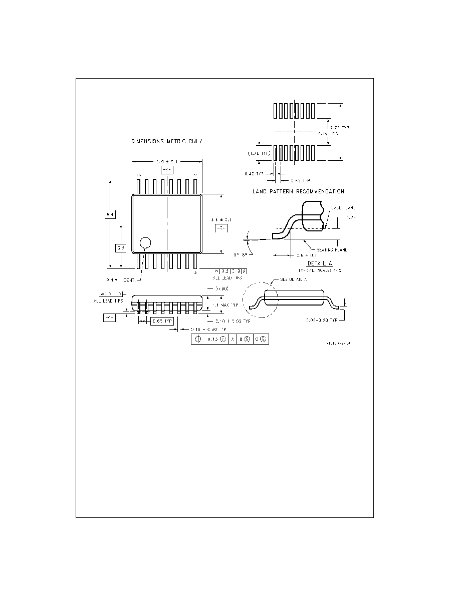
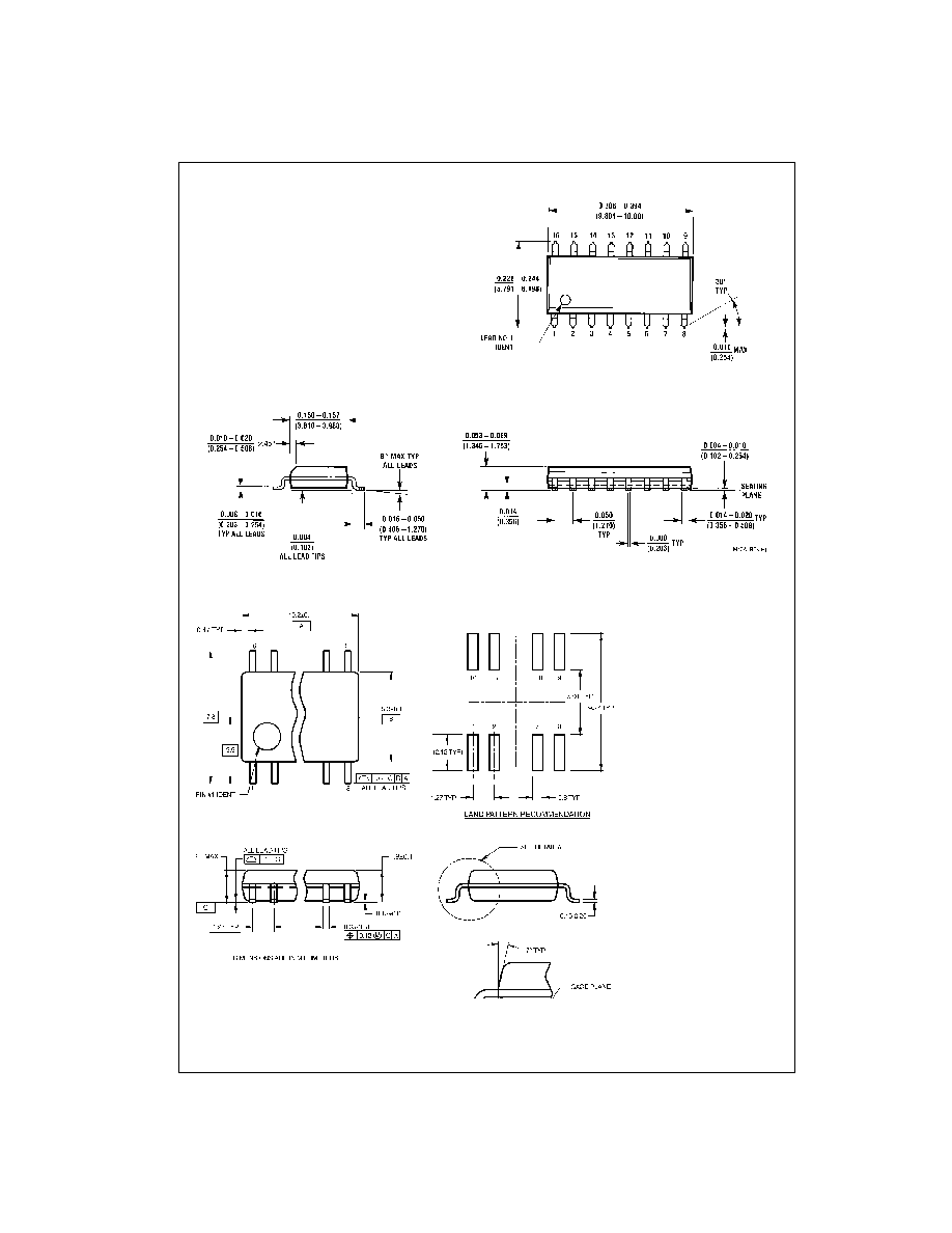
Physical Dimensions
inches (millimeters) unless otherwise noted
16-Lead Small Outline Integrated Circuit (SOIC), JEDEC MS-012, 0.150" Narrow
Package Number M16A
16-Lead Small Outline Package (SOP), EIAJ TYPE II, 5.3mm Wide
Package Number M16D