August 1984
Revised May 1999
MM74HC4051
∑
MM74HC4052 ∑
MM74HC4053 8-Channel
A
n
a
l
og Mult
ipl
exer ∑
© 1999 Fairchild Semiconductor Corporation
DS005353.prf
www.fairchildsemi.com
MM74HC4051 ∑ MM74HC4052 ∑ MM74HC4053
8-Channel Analog Multiplexer ∑
Dual 4-Channel Analog Multiplexer ∑
Triple 2-Channel Analog Multiplexer
General Description
The MM74HC4051, MM74HC4052 and MM74HC4053
multiplexers are digitally controlled analog switches imple-
mented in advanced silicon-gate CMOS technology. These
switches have low "on" resistance and low "off" leakages.
They are bidirectional switches, thus any analog input may
be used as an output and vice-versa. Also these switches
contain linearization circuitry which lowers the on resis-
tance and increases switch linearity. These devices allow
control of up to
±
6V (peak) analog signals with digital con-
trol signals of 0 to 6V. Three supply pins are provided for
V
CC
, ground, and V
EE
. This enables the connection of 0≠
5V logic signals when V
CC
=
5V and an analog input range
of
±
5V when V
EE
=
5V. All three devices also have an
inhibit control which when HIGH will disable all switches to
their off state. All analog inputs and outputs and digital
inputs are protected from electrostatic damage by diodes
to V
CC
and ground.
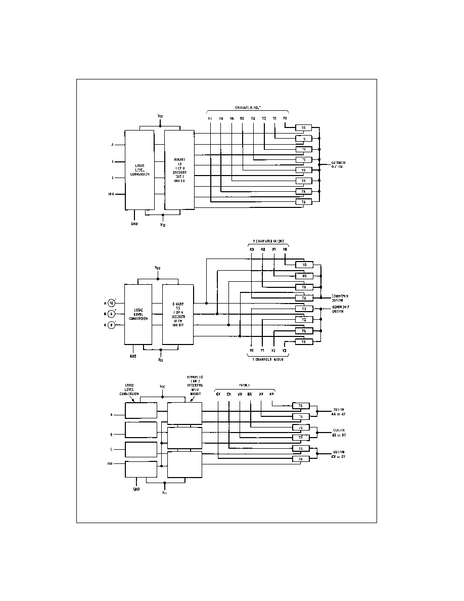
MM74HC4051: This device connects together the outputs
of 8 switches, thus achieving an 8 channel Multiplexer. The
binary code placed on the A, B, and C select lines deter-
mines which one of the eight switches is "on", and con-
nects one of the eight inputs to the common output.
MM74HC4052: This device connects together the outputs
of 4 switches in two sets, thus achieving a pair of 4-channel
multiplexers. The binary code placed on the A, and B
select lines determine which switch in each 4 channel sec-
tion is "on", connecting one of the four inputs in each sec-
tion to its common output. This enables the implementation
of a 4-channel differential multiplexer.
MM74HC4053: This device contains 6 switches whose out-
puts are connected together in pairs, thus implementing a
triple 2 channel multiplexer, or the equivalent of 3 single-
pole-double throw configurations. Each of the A, B, or C
select lines independently controls one pair of switches,
selecting one of the two switches to be "on".
Features
s
Wide analog input voltage range:
±
6V
s
Low "on" resistance:
50 typ. (V
CC
≠V
EE
=
4.5V)
30 typ. (V
CC
≠V
EE
=
9V)
s
Logic level translation to enable 5V logic with
±
5V ana-
log signals
s
Low quiescent current: 80
µ
A maximum (74HC)
s
Matched Switch characteristic
Ordering Code:
Devices also available in Tape and Reel. Specify by appending the suffix letter "X" to the ordering code.
Order Number
Package Number
Package Description
MM74HC4051M
M16A
16-Lead Small Outline Integrated Circuit (SOIC), JEDEC MS-012, 0.150" Narrow
MM74HC4051WM
M16B
16-Lead Small Outline Integrated Circuit (SOIC), JEDEC MS-013, 0.300" Wide
MM74HC4051SJ
M16D
16-Lead Small Outline Package (SOP), EIAJ TYPE II, 5.3mm Wide
MM74HC4051MTC
MTC16
16-Lead Thin Shrink Small Outline Package (TSSOP), JEDEC MO-153, 4.4mm Wide
MM74HC4051N
N16E
16-Lead Plastic Dual-In-Line Package (PDIP), JEDEC MS-0010.300" Wide
MM74HC4052M
M16A
16-Lead Small Outline Integrated Circuit (SOIC), JEDEC MS-012, 0.150" Narrow
MM74HC4052WM
M16B
16-Lead Small Outline Integrated Circuit (SOIC), JEDEC MS-013, 0.300" Wide
MM74HC4052SJ
M16D
16-Lead Small Outline Package (SOP), EIAJ TYPE II, 5.3mm Wide
MM74HC4052MTC
MTC16
16-Lead Thin Shrink Small Outline Package (TSSOP), JEDEC MO-153, 4.4mm Wide
MM74HC4052N
N16E
16-Lead Plastic Dual-In-Line Package (PDIP), JEDEC MS-0010.300" Wide
MM74HC4053M
M16A
16-Lead Small Outline Integrated Circuit (SOIC), JEDEC MS-012, 0.150" Narrow
MM74HC4053WM
M16B
16-Lead Small Outline Integrated Circuit (SOIC), JEDEC MS-013, 0.300" Wide
MM74HC4053SJ
M16D
16-Lead Small Outline Package (SOP), EIAJ TYPE II, 5.3mm Wide
MM74HC4053MTC
MTC16
16-Lead Thin Shrink Small Outline Package (TSSOP), JEDEC MO-153, 4.4mm Wide
MM74HC4053N
N16E
16-Lead Plastic Dual-In-Line Package (PDIP), JEDEC MS-0010.300" Wide

www.fairchildsemi.com
4
MM
7
4
HC
4
051
∑ MM
74
H
C
40
52
∑ M
M
74HC4053
Absolute Maximum Ratings
(Note 1)
(Note 2)
Recommended Operating
Conditions
Note 1: Absolute Maximum Ratings are those values beyond which dam-
age to the device may occur.
Note 2: Unless otherwise specified all voltages are referenced to ground.
Note 3: Power Dissipation temperature derating -- plastic "N" package:
-
12 mW/
∞
C from 65
∞
C to 85
∞
C.
DC Electrical Characteristics
(Note 4)
Supply Voltage (V
CC
)
-
0.5 to
+
7.5V
Supply Voltage (V
EE
)
+
0.5 to
-
7.5V
Control Input Voltage (V
IN
)
-
1.5 to V
CC
+
1.5V
Switch I/O Voltage (V
IO
)
V
EE
-
0.5 to V
CC
+
0.5V
Clamp Diode Current (I
IK
, I
OK
)
±
20 mA
Output Current, per pin (I
OUT
)
±
25 mA
V
CC
or GND Current, per pin (I
CC
)
±
50 mA
Storage Temperature Range (T
STG
)
-
65
∞
C to
+
150
∞
C
Power Dissipation (P
D
)
(Note 3)
600 mW
S.O. Package only
500 mW
Lead Temperature (T
L
)
(Soldering 10 seconds)
260
∞
C
Min
Max
Units
Supply Voltage (V
CC
)
2
6
V
Supply Voltage (V
EE
)
0
-
6
V
DC Input or Output Voltage
(V
IN
, V
OUT
)
0
V
CC
V
Operating Temperature Range (T
A
)
-
40
+
85
∞
C
Input Rise or Fall Times
(t
r
, t
f
) V
CC
=
2.0V
1000
ns
V
CC
=
4.5V
500
ns
V
CC
=
6.0V
400
ns
Symbol
Parameter
Conditions
V
EE
V
CC
T
A
=
25
∞
C
T
A
=
-
40 to 85
∞
C T
A
=
-
55 to 125
∞
C
Units
Typ
Guaranteed Limits
V
IH
Minimum HIGH Level
2.0V
1.5
1.5
1.5
V
Input Voltage
4.5V
3.15
3.15
3.15
V
6.0V
4.2
4.2
4.2
V
V
IL
Maximum LOW Level
2.0V
0.5
0.5
0.5
V
Input Voltage
4.5V
1.35
1.35
1.35
V
6.0V
1.8
1.8
1.8
V
R
ON
Maximum "ON" Resistance
V
INH
=
V
IL
, I
S
=
2.0 mA
GND
4.5V
40
160
200
240
(Note 5)
V
IS
=
V
CC
to V
EE
-
4.5V 4.5V
30
120
150
170
(Figure 1)
-
6.0V 6.0V
20
100
125
140
V
INH
=
V
IL
, I
S
=
2.0 mA
GND
2.0V
100
230
280
320
V
IS
=
V
CC
or V
EE
GND
4.5V
40
110
140
170
(Figure 1)
-
4.5V 4.5V
20
90
120
140
-
6.0V 6.0V
15
80
100
115
R
ON
Maximum "ON" Resistance
V
CTL
=
V
IL
GND
4.5V
10
20
25
25
Matching
V
IS
=
V
CC
to GND
-
4.5V 4.5V
5
10
15
15
-
6.0V 6.0V
5
10
12
15
I
IN
Maximum Control
V
IN
=
V
CC
or GND
±
0.1
±
1.0
±
1.0
µ
A
Input Current
V
CC
=
2
-
6V
I
CC
Maximum Quiescent
V
IN
=
V
CC
or GND
GND
6.0V
8
80
160
µ
A
Supply Current
I
OUT
=
0
µ
A
-
6.0V 6.0V
16
160
320
µ
A
I
IZ
Maximum Switch "OFF"
V
OS
=
V
CC
or V
EE
GND
6.0V
±
60
±
600
±
600
nA
Leakage Current
V
IS
=
V
EE
or V
CC
-
6.0V 6.0V
±
100
±
1000
±
1000
nA
(Switch Input)
V
INH
=
V
IH
(Figure 2)
I
IZ
Maximum Switch
V
IS
=
V
CC
to V
EE
GND
6.0V
±
0.2
±
2.0
±
2.0
µ
A
"ON" Leakage
HC4051 V
INH
=
V
IL
-
6.0V 6.0V
±
0.4
±
4.0
±
4.0
µ
A
Current
(Figure 3)
V
IS
=
V
CC
to V
EE
GND
6.0V
±
0.1
±
1.0
±
1.0
µ
A
HC4052 V
INH
=
V
IL
(Figure 3)
-
6.0V 6.0V
±
0.2
±
2.0
±
2.0
µ
A
V
IS
=
V
CC
to V
EE
GND
6.0V
±
0.1
±
1.0
±
1.0
µ
A
HC4053 V
INH
=
V
IL
(Figure 3)
-
6.0V 6.0V
±
0.1
±
1.0
±
1.0
µ
A

5
www.fairchildsemi.com
MM74HC4051
∑ MM74HC4052
∑ MM74HC4053
DC Electrical Characteristics
(Continued)
Note 4: For a power supply of 5V
±
10% the worst case on resistances (R
ON
) occurs for HC at 4.5V. Thus the 4.5V values should be used when designing
with this supply. Worst case V
IH
and V
IL
occur at V
CC
=
5.5V and 4.5V respectively. (The V
IH
value at 5.5V is 3.85V.) The worst case leakage current occur
for CMOS at the higher voltage and so the 5.5V values should be used.
Note 5: At supply voltages (V
CC
≠V
EE
) approaching 2V the analog switch on resistance becomes extremely non-linear. Therefore it is recommended that
these devices be used to transmit digital only when using these supply voltages.
AC Electrical Characteristics
V
CC
=
2.0V
-
6.0V, V
EE
=
0V
-
6V, C
L
=
50 pF (unless otherwise specified)
Symbol
Parameter
Conditions
V
EE
V
CC
T
A
=
25
∞
C
T
A
=
-
40 to 85
∞
C T
A
=
-
55 to 125
∞
C
Units
Typ
Guaranteed Limits
I
IZ
Maximum Switch
V
OS
=
V
CC
or V
EE
GND
6.0V
±
0.2
±
2.0
±
2.0
µ
A
"OFF" Leakage
HC4051 V
IS
=
V
EE
or V
CC
-
6.0V 6.0V
±
0.4
±
4.0
±
4.0
µ
A
Current (Common Pin)
V
INH
=
V
IH
V
OS
=
V
CC
or V
EE
GND
6.0V
±
0.1
±
1.0
±
1.0
µ
A
HC4052 V
IS
=
V
EE
or V
CC
-
6.0V 6.0V
±
0.2
±
2.0
±
2.0
µ
A
V
INH
=
V
IH
V
OS
=
V
CC
or V
EE
GND
6.0V
±
0.1
±
1.0
±
1.0
µ
A
HC4053 V
IS
=
V
EE
or V
CC
-
6.0V 6.0V
±
0.1
±
1.0
±
1.0
µ
A
V
INH
=
V
IH
Symbol
Parameter
Conditions
V
EE
V
CC
T
A
=
25
∞
C
T
A
=
-
40 to 85
∞
C T
A
=
-
55 to 125
∞
C
Units
Typ
Guaranteed Limits
t
PHL
, t
PLH
Maximum Propagation
GND
2.0V
25
60
75
90
ns
Delay Switch In to Out
GND
4.5V
5
12
15
18
ns
-
4.5V
4.5V
4
8
12
14
ns
-
6.0V
6.0V
3
7
11
13
ns
t
PZL
, t
PZH
Maximum Switch Turn
R
L
=
1 k
GND
2.0V
92
355
435
515
ns
"ON" Delay
GND
4.5V
69
87
103
ns
-
4.5V
4.5V
16
46
58
69
ns
-
6.0V
6.0V
15
41
51
62
ns
t
PHZ
, t
PLZ
Maximum Switch Turn
GND
2.0V
65
290
365
435
ns
"OFF" Delay
GND
4.5V
28
58
73
87
ns
-
4.5V
4.5V
18
37
46
56
ns
-
6.0V
6.0V
16
32
41
48
ns
f
MAX
Minimum Switch
GND
4.5V
30
MHz
Frequency Response
-
4.5V
4.5V
35
MHz
20 log (V
I
/V
O
)
=
3 dB
Control to Switch
R
L
=
600
,
V
IS
=
4 V
PP
0V
4.5V
1080
mV
Feedthrough Noise
f
=
1 MHz,
V
IS
=
8 V
PP
-
4.5V
4.5V
250
mV
C
L
=
50 pF
Crosstalk between
R
L
=
600
,
V
IS
=
4 V
PP
0V
4.5
-
52
dB
any Two Switches
f
=
1 MHz
V
IS
=
8 V
PP
-
4.5V
4.5V
-
50
dB
Switch OFF Signal
R
L
=
600
,
V
IS
=
4 V
PP
0V
4.5V
-
42
dB
Feedthrough
f
=
1 MHz,
V
IS
=
8 V
PP
-
4.5V
4.5V
-
44
dB
Isolation
V
CTL
=
V
IL
THD
Sinewave Harmonic
R
L
=
10 k
,
V
IS
=
4 V
PP
0V
4.5V
0.013
%
Distortion
C
L
=
50 pF,
V
IS
=
8 V
PP
-
4.5V
4.5V
0.008
%
f
=
1 kHz
C
IN
Maximum Control
5
10
10
10
pF
Input Capacitance
C
IN
Maximum Switch
Input
15
pF
Input Capacitance
4051 Common
90
4052 Common
45
4053 Common
30
C
IN
Maximum Feedthrough
Capacitance
5
pF