Äîêóìåíòàöèÿ è îïèñàíèÿ www.docs.chipfind.ru
August 1984
Revised February 1999
MM74HC4060 14 S
t
a
g
e Binary
Cou
n
ter
© 1999 Fairchild Semiconductor Corporation
DS005354.prf
www.fairchildsemi.com
MM74HC4060
14 Stage Binary Counter
General Description
The MM74HC4060 is a high speed binary ripple carry
counter. These counters are implemented utilizing
advanced silicon-gate CMOS technology to achieve speed
performance similar to LS-TTL logic while retaining the low
power and high noise immunity of CMOS.
The MM74HC4060 is a 14-stage counter, which device
increments on the falling edge (negative transition) of the
input clock, and all their outputs are reset to a low level by
applying a logical high on their reset input. The
MM74HC4060 also has two additional inputs to enable
easy connection of either an RC or crystal oscillator.
This device is pin equivalent to the CD4060. All inputs are
protected from damage due to static discharge by protec-
tion diodes to V
CC
and ground.
Features
s
Typical propagation delay: 16 ns
s
Wide operating voltage range: 26V
s
Low input current: 1
µ
A maximum
s
Low quiescent current: 80
µ
A maximum (74 Series)
s
Output drive capability: 10 LS-TTL loads
Ordering Code:
Devices also available in Tape and Reel. Specify by appending the suffix letter "X" to the ordering code.
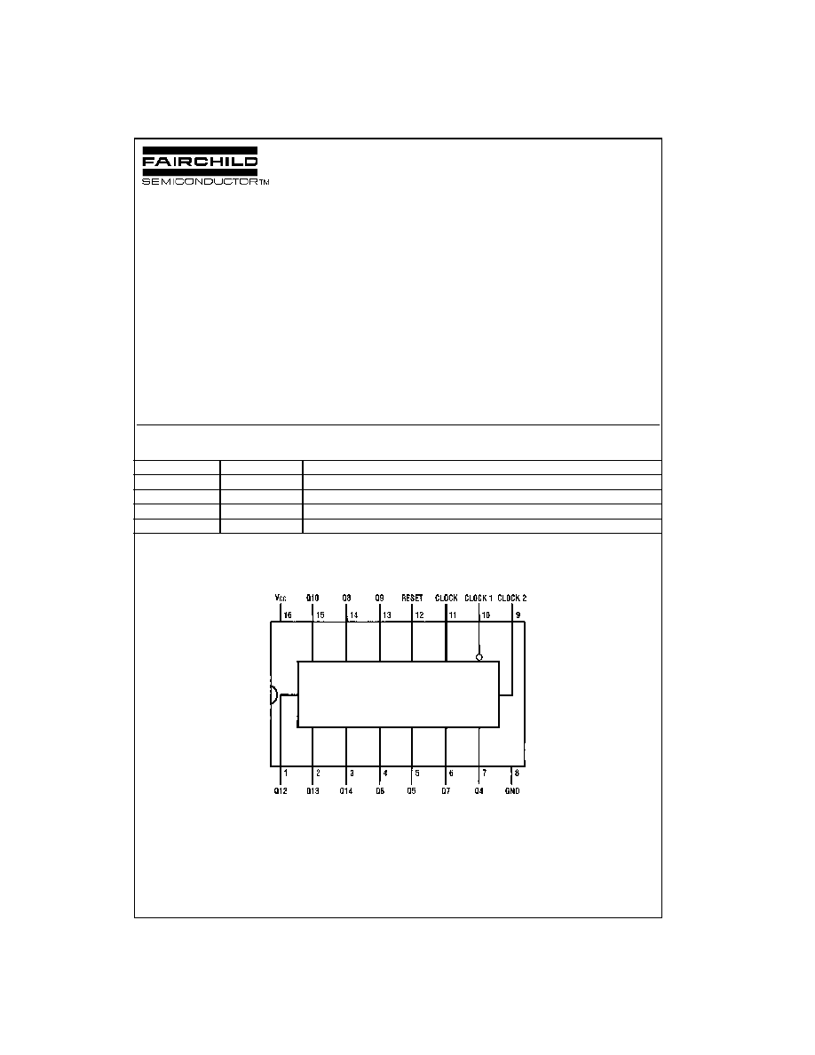
Connection Diagram
Pin Assignments for DIP, SOIC, SOP and TSSOP
Top View
Order Number
Package Number
Package Description
MM74HC4060M
M16A
16-Lead Small Outline Integrated Circuit (SOIC), JEDEC MS-012, 0.150" Narrow
MM74HC4060SJ
M16D
16-Lead Small Outline Package (SOP), EIAJ TYPE II, 5.3mm Wide
MM74HC4060MTC
MTC16
16-Lead Thin Shrink Small Outline Package (TSSOP), JEDEC MO-153, 4.4mm Wide
MM74HC4060N
N16E
16-Lead Plastic Dual-In-Line Package (PDIP), JEDEC MS-001, 0.300" Wide
www.fairchildsemi.com
2
M
M
74HC4060
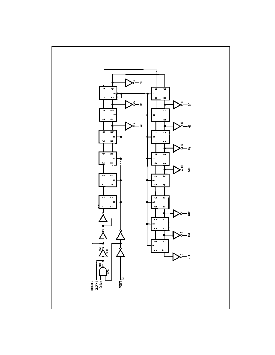
Logic Diagram
3
www.fairchildsemi.com
MM74HC4060
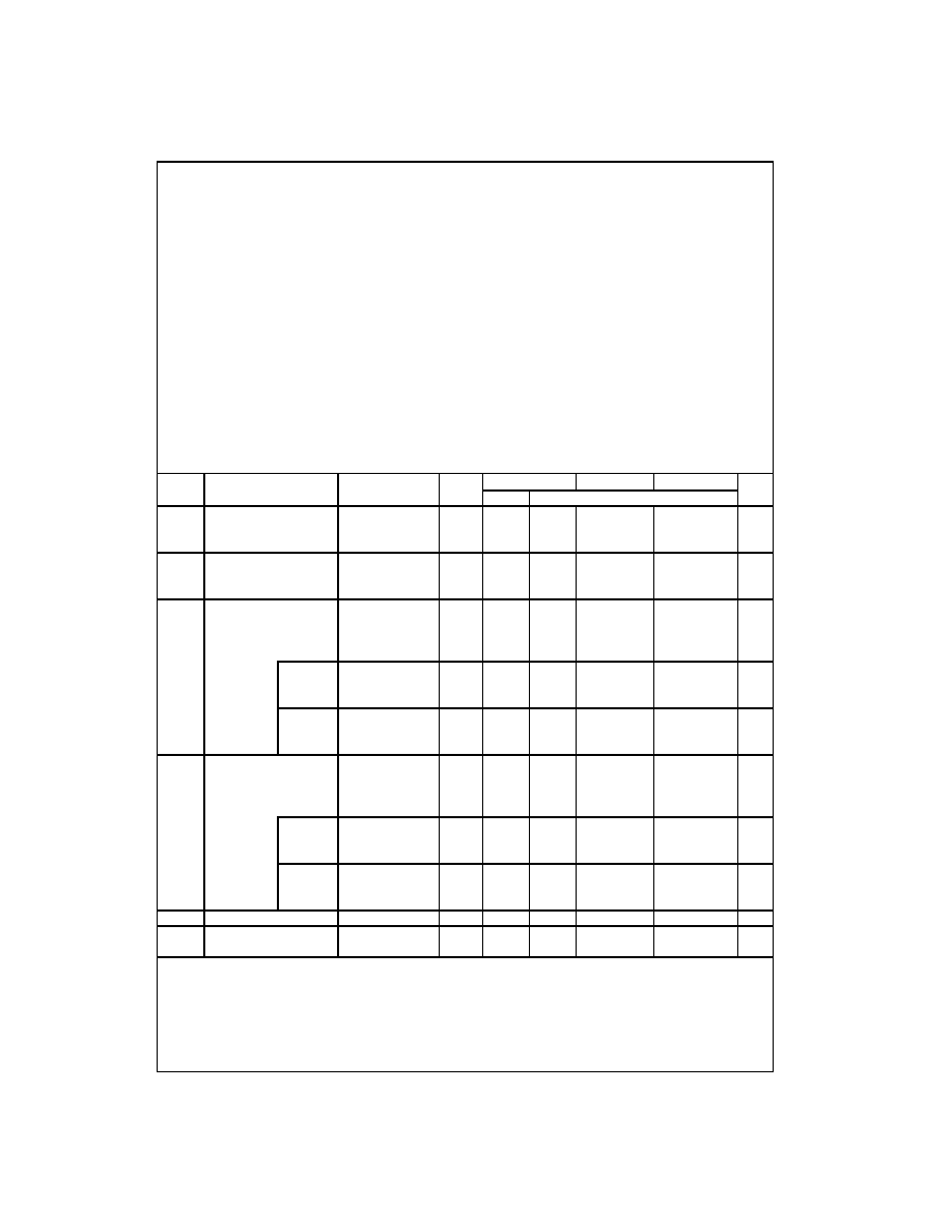
Absolute Maximum Ratings
(Note 1)
(Note 2)
Recommended Operating
Conditions
Note 1: Maximum Ratings are those values beyond which damage to the
device may occur.
Note 2: Unless otherwise specified all voltages are referenced to ground.
Note 3: Power Dissipation temperature derating: plastic "N" package:
-
12 mW/
°
C from 65
°
C to 85
°
C.
DC Electrical Characteristics
(Note 4)
Note 4: For a power supply of 5V
±
10% the worst case output voltages (V
OH
, and V
OL
) occur for HC at 4.5V. Thus the 4.5V values should be used when
designing with this supply. Worst case V
IH
and V
IL
occur at V
CC
=
5.5V and 4.5V respectively. (The V
IH
value at 5.5V is 3.85V.) The worst case leakage cur-
rent (I
IN
, I
CC
, and I
OZ
) occur for CMOS at the higher voltage and so the 6.0V values should be used.
Supply Voltage (V
CC
)
-
0.5 to
+
7.0V
DC Input Voltage (V
IN
)
-
1.5 to V
CC
+
1.5V
DC Output Voltage (V
OUT
)
-
0.5 to V
CC
+
0.5V
Clamp Diode Current (I
CD
)
±
20 mA
DC Output Current, per pin (I
OUT
)
±
25 mA
DC V
CC
or GND Current, per pin (I
CC
)
±
50 mA
Storage Temperature Range (T
STG
)
-
65
°
C to
+
150
°
C
Power Dissipation (P
D
)
(Note 3)
600 mW
S.O. Package only
500 mW
Lead Temperature (T
L
)
(Soldering 10 seconds)
260
°
C
Min
Max
Units
Supply Voltage (V
CC
)
2
6
V
DC Input or Output Voltage
(V
IN
, V
OUT
)
0
V
CC
V
Operating Temperature Range (T
A
)
-
40
+
85
°
C
Input Rise or Fall Times
(t
r
, t
f
) V
CC
=
2.0V
1000
ns
V
CC
=
4.5V
500
ns
V
CC
=
6.0V
400
ns
Symbol
Parameter
Conditions
V
CC
T
A
=
25
°
C
T
A
=
-
40 to 85
°
C T
A
=
-
55 to 125
°
C
Units
Typ
Guaranteed Limits
V
IH
Minimum
HIGH 2.0V
1.5
1.5
1.5
V
Level
Voltage 4.5V
3.15
3.15
3.15
V
(Not Applicable to Pins 9 & 10)
6.0V
4.2
4.2
4.2
V
V
IL
Maximum LOW Level
2.0V
0.5
0.5
0.5
V
Input Voltage
4.5V
1.35
1.35
1.35
V
(Not Applicable to Pins 9 & 10)
6.0V
1.8
1.8
1.8
V
V
OH
Minimum HIGH Level
V
IN
=
V
IH
or V
IL
Output Voltage
|I
OUT
|
20
µ
A
2.0V
2.0
1.9
1.9
1.9
V
4.5V
4.5
4.4
4.4
4.4
V
6.0V
6.0
5.9
5.9
5.9
V
Except Pins
V
IN
=
V
IH
or V
IL
9 & 10
|I
OUT
|
4.0 mA
4.5V
4.2
3.98
3.84
3.7
V
|I
OUT
|
5.2 mA
6.0V
5.7
5.48
5.34
5.2
V
Pins
V
IN
=
V
IH
or V
IL
3.98
3.84
3.7
V
9 & 10
|I
OUT
|
=
0.4 mA
5.48
5.34
5.2
V
|I
OUT
|
=
0.52 mA
V
OL
Maximum LOW Level
V
IN
=
V
IH
or V
IL
Output Voltage
|I
OUT
|
20
µ
A
2.0V
0
0.1
0.1
0.1
V
4.5V
0
0.1
0.1
0.1
V
6.0V
0
0.1
0.1
0.1
V
Except Pins
V
IN
=
V
IH
or V
IL
9 & 10
|I
OUT
|
4.0 mA
4.5V
0.2
0.26
0.33
0.4
V
|I
OUT
|
5.2 mA
6.0V
0.2
0.26
0.33
0.4
V
Pins
V
IN
=
V
IH
or V
IL
0.26
0.33
0.4
V
9 & 10
|I
OUT
|
=
0.4 mA
0.26
0.33
0.4
V
|I
OUT
|
=
0.52 mA
I
IN
Maximum Input Current
V
IN
=
V
CC
or GND
6.0V
±
0.1
±
1.0
±
1.0
µ
A
I
CC
Maximum Quiescent
V
IN
=
V
CC
or GND
Supply Current
I
OUT
=
0
µ
A
6.0V
8.0
80
160
µ
A
www.fairchildsemi.com
4
M
M
74HC4060
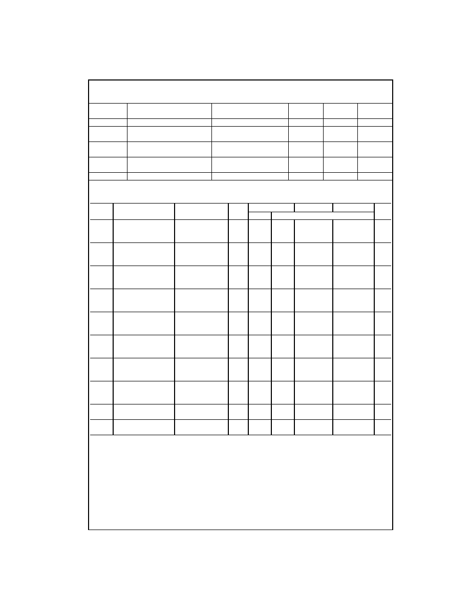
AC Electrical Characteristics
V
CC
=
5V, T
A
=
25
°
C, C
L
=
15 pF, t
r
=
t
f
=
6 ns
AC Electrical Characteristics
V
CC
=
2.0V to 6.0V, C
L
=
50 pF, t
r
=
t
f
=
6 ns (unless otherwise specified)
Note 5: Typical Propagation delay time to any output can be calculated using: t
P
=
17
+
12(N1) ns; where N is the number of the output, Q
W
, at V
CC
=
5V.
Note 6: C
PD
determines the no load dynamic power consumption, P
D
=
C
PD
V
CC
2
f
+
I
CC
V
CC
, and the no load dynamic current consumption,
I
S
=
C
PD
V
CC
f
+
I
CC
.
Symbol
Parameter
Conditions
Typ
Guaranteed
Units
Limit
f
MAX
Maximum Clock Frequency
30
MHz
t
PHL
, t
PLH
Maximum Propagation
(Note 5)
40
20
ns
Delay to Q
4
t
PHL
, t
PLH
Maximum Propagation
16
40
ns
Delay to any Q
t
REM
Minimum Reset
10
20
ns
Removal Time
t
W
Minimum Pulse Width
10
16
ns
Symbol
Parameter
Conditions
V
CC
T
A
=
25
°
C
T
A
=
-
40 to 85
°
C T
A
=
-
55 to 125
°
C
Units
Typ
Guaranteed Limits
f
MAX
Maximum Operating
2.0V
6
5
4
MHz
Frequency
4.5V
30
24
20
MHz
6.0V
35
28
24
MHz
t
PHL
, t
PLH
Maximum Propagation
2.0V
120
380
475
171
ns
Delay Clock to Q
4
4.5V
42
76
95
114
ns
6.0V
35
65
81
97
ns
t
PHL
Maximum Propagation
2.0V
72
240
302
358
ns
Delay Reset to any Q
4.5V
24
48
60
72
ns
6.0V
20
41
51
61
ns
t
PHL
, t
PLH
Maximum Propagation
2.0V
125
156
188
ns
Delay Between Stages
4.5V
25
31
38
ns
Q
n
to Q
n
+
1
6.0V
21
26
31
ns
t
REM
Minimum Reset
2.0V
100
125
150
ns
Removal Time
4.5V
20
25
30
ns
6.0V
17
21
25
ns
t
W
Minimum Pulse Width
2.0V
80
100
120
ns
4.5V
16
20
24
ns
6.0V
14
17
20
ns
t
r
, t
f
Maximum Input Rise and
2.0V
1000
1000
1000
ns
Fall Time
4.5V
500
500
500
ns
6.0V
400
400
400
ns
t
THL
, t
TLH
Maximum Output Rise
2.0V
30
75
95
110
ns
and Fall Time
4.5V
10
15
19
22
ns
6.0V
9
13
16
19
ns
C
PD
Power Dissipation
(per package)
55
pF
Capacitance (Note 6)
C
IN
Maximum Input
5
10
10
10
pF
Capacitance
5
www.fairchildsemi.com
MM74HC4060
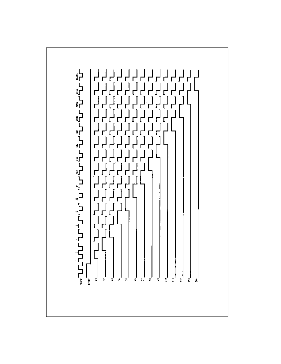
Timing Diagram
www.fairchildsemi.com
6
M
M
74HC4060
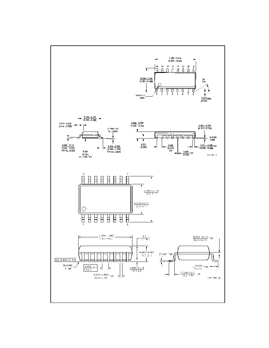
Physical Dimensions
inches (millimeters) unless otherwise noted
16-Lead Small Outline Integrated Circuit (SOIC), JEDEC MS-012, 0.150" Narrow
Package Number M16A
16-Lead Small Outline Package (SOP), EIAJ TYPE II, 5.3mm Wide
Package Number M16D
7
www.fairchildsemi.com
MM74HC4060
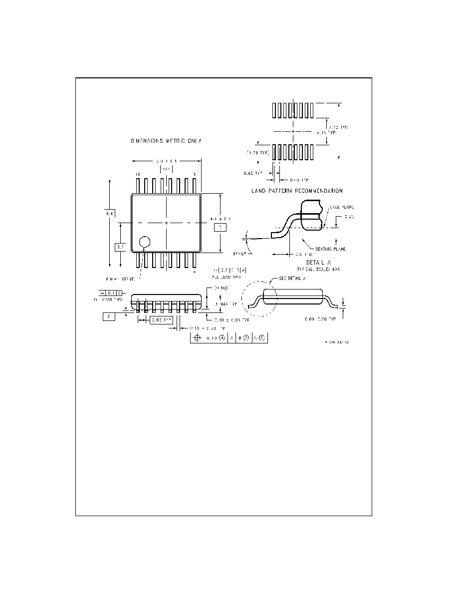
Physical Dimensions
inches (millimeters) unless otherwise noted (Continued)
16-Lead Thin Shrink Small Outline Package (TSSOP), JEDEC MO-153, 4.4mm Wide
Package Number MTC16
Fairchild does not assume any responsibility for use of any circuitry described, no circuit patent licenses are implied and Fairchild reserves the right at any time without notice to change said circuitry and specifications.
MM74HC4060 14 S
t
a
g
e Binary C
o
u
n
ter
LIFE SUPPORT POLICY
FAIRCHILD'S PRODUCTS ARE NOT AUTHORIZED FOR USE AS CRITICAL COMPONENTS IN LIFE SUPPORT
DEVICES OR SYSTEMS WITHOUT THE EXPRESS WRITTEN APPROVAL OF THE PRESIDENT OF FAIRCHILD
SEMICONDUCTOR CORPORATION. As used herein:
1. Life support devices or systems are devices or systems
which, (a) are intended for surgical implant into the
body, or (b) support or sustain life, and (c) whose failure
to perform when properly used in accordance with
instructions for use provided in the labeling, can be rea-
sonably expected to result in a significant injury to the
user.
2. A critical component in any component of a life support
device or system whose failure to perform can be rea-
sonably expected to cause the failure of the life support
device or system, or to affect its safety or effectiveness.
www.fairchildsemi.com
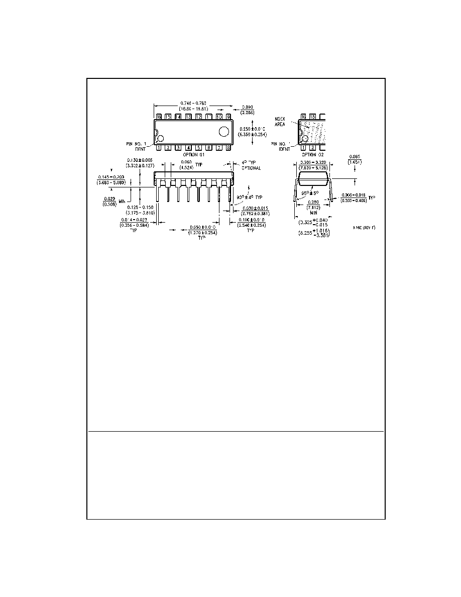
Physical Dimensions
inches (millimeters) unless otherwise noted (Continued)
16-Lead Plastic Dual-In-Line Package (PDIP), JEDEC MS-001, 0.300" Wide
Package Number N16E