Äîêóìåíòàöèÿ è îïèñàíèÿ www.docs.chipfind.ru
February 1984
Revised February 1999
MM74HCT373
· MM74HCT374
3-ST
A
T
E Oct
a
l
D-T
ype L
a
tc
h
· 3-
ST
A
T
E
Octal
D-
T
ype
Fl
ip-
F
lop
© 1999 Fairchild Semiconductor Corporation
DS005367.prf
www.fairchildsemi.com
MM74HCT373 · MM74HCT374
3-STATE Octal D-Type Latch ·
3-STATE Octal D-Type Flip-Flop
General Description
The MM74HCT373 octal D-type latches and
MM74HCT374 Octal D-type flip flops advanced silicon-
gate CMOS technology, which provides the inherent bene-
fits of low power consumption and wide power supply
range, but are LS-TTL input and output characteristic &
pin-out compatible. The 3-STATE outputs are capable of
driving 15 LS-TTL loads. All inputs are protected from dam-
age due to static discharge by internal diodes to V
CC
and
ground.
When the MM74HCT373 LATCH ENABLE input is HIGH,
the Q outputs will follow the D inputs. When the LATCH
ENABLE goes LOW, data at the D inputs will be retained at
the outputs until LATCH ENABLE returns HIGH again.
When a high logic level is applied to the OUTPUT CON-
TROL input, all outputs go to a high impedance state,
regardless of what signals are present at the other inputs
and the state of the storage elements.
The MM74HCT374 are positive edge triggered flip-flops.
Data at the D inputs, meeting the setup and hold time
requirements, are transferred to the Q outputs on positive
going transitions of the CLOCK (CK) input. When a high
logic level is applied to the OUTPUT CONTROL (OC)
input, all outputs go to a high impedance state, regardless
of what signals are present at the other inputs and the state
of the storage elements.
MM74HCT devices are intended to interface between TTL
and NMOS components and standard CMOS devices.
These parts are also plug in replacements for LS-TTL
devices and can be used to reduce power consumption in
existing designs.
Features
s
TTL input characteristic compatible
s
Typical propagation delay: 20 ns
s
Low input current: 1
µ
A maximum
s
Low quiescent current: 80
µ
A maximum
s
Compatible with bus-oriented systems
s
Output drive capability: 15 LS-TTL loads
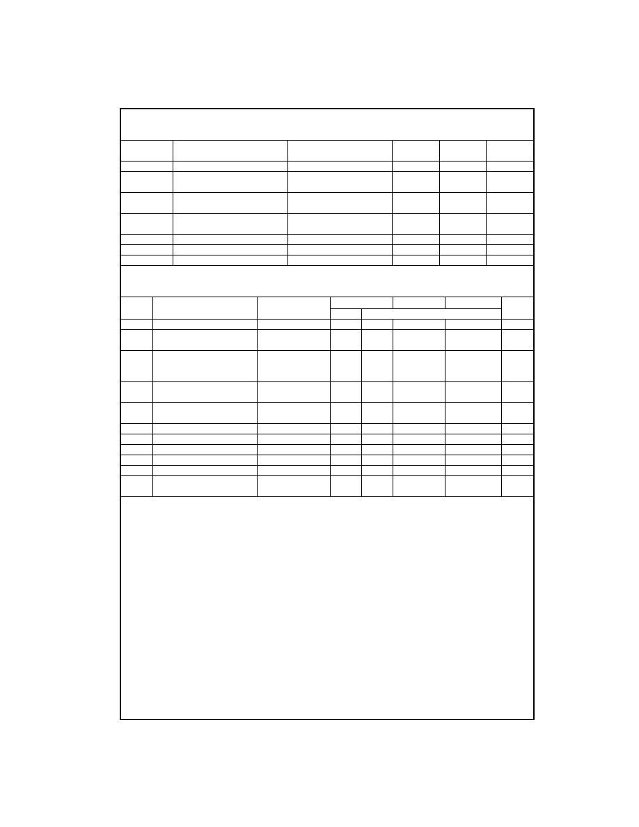
Ordering Code:
Devices also available in Tape and Reel. Specify by appending the suffix letter "X" to the ordering code.
Order Number
Package Number
Package Descriptions
MM74HCT373WM
M20B
20-Lead Small Outline Integrated Circuit (SOIC), JEDEC MS-013, 0.300" Wide
MM74HCT373SJ
M20D
20-Lead Small Outline Package (SOP), EIAJ TYPE II, 5.3mm Wide
MM74HCT373MTC
MTC20
20-Lead Thin Shrink Small Outline Package (TSSOP), JEDEC MO-153, 4.4mm Wide
MM74HCT373N
N20A
20-Lead Plastic Dual-In-Line Package (PDIP), JEDEC MS-001, 0.300" Wide

www.fairchildsemi.com
2
MM
74
H
C
T3
73
· MM
74HCT374
Connection Diagrams
Pin Assignments for DIP, SOIC, SOP and TSSOP
Top View
MM74HCT373
Top View
MM74HCT374
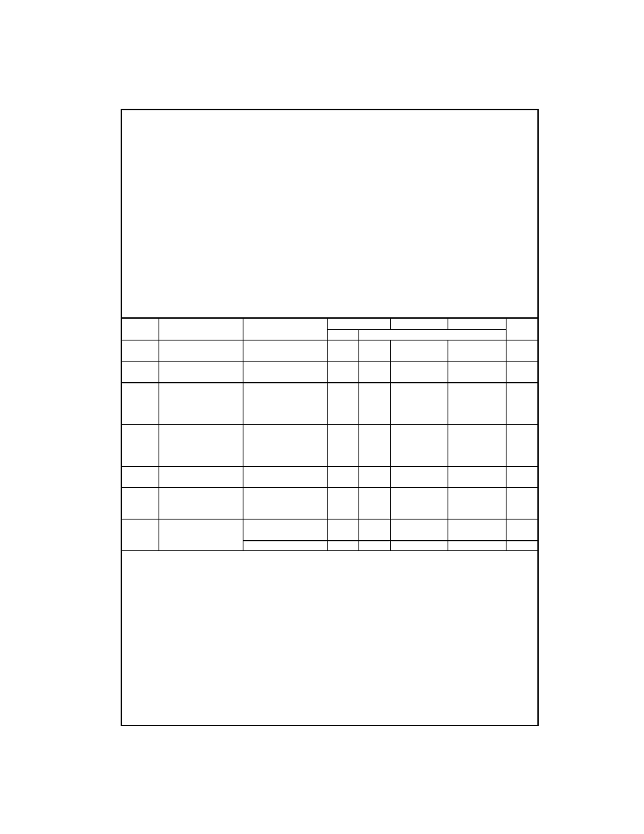
Truth Tables
MM74HCT373
H
=
HIGH Level
L
=
LOW Level
Q
0
=
Level of output before steady-state input conditions were established.
Z
=
High Impedance
MM74HCT374
H
=
HIGH Level
L
=
LOW Level
X
=
Don't Care
=
Transition from LOW-to-HIGH
Z
=
High Impedance State
Q
0
=
The level of the output before steady state input conditions were
established.
Output
LE
Data
373
Control
Output
L
H
H
H
L
H
L
L
L
L
X
Q
0
H
X
X
Z
Output
Clock
Data
Output
Control
(374)
L
H
H
L
L
L
L
L
X
Q
0
H
X
X
Z
3
www.fairchildsemi.com
MM74HCT373
· MM74HCT374
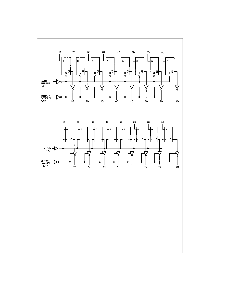
Logic Diagrams
MM74HCT373
MM74HCT374
www.fairchildsemi.com
4
MM
74
H
C
T3
73
· MM
74HCT374
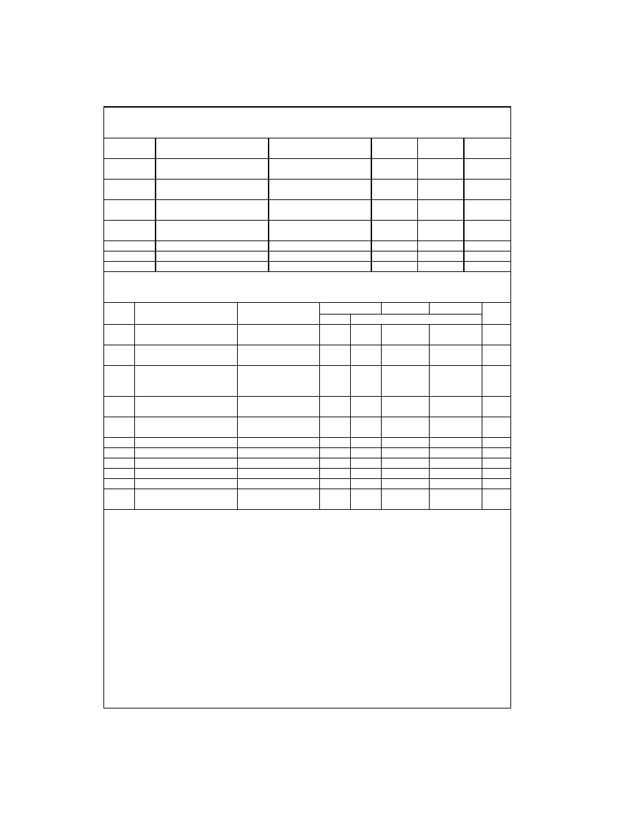
Absolute Maximum Ratings
(Note 1)
(Note 2)
Recommended Operating
Conditions
Note 1: Absolute Maximum Ratings are those values beyond which dam-
age to the device may occur.
Note 2: Unless otherwise specified all voltages are referenced to ground.
Note 3: Power Dissipation temperature derating -- plastic "N" package:
-
12 mW/
°
C from 65
°
C to 85
°
C.
DC Electrical Characteristics
V
CC
=
5V
±
10% (unless otherwise specified)
Note 4: Measured per pin. All others tied to V
CC
or ground.
Supply Voltage (V
CC
)
-
0.5 to
+
7.0V
DC Input Voltage (V
IN
)
-
1.5 to V
CC
+
1.5V
DC Output Voltage (V
OUT
)
-
0.5 to V
CC
+
0.5V
Clamp Diode Current (I
IK
, I
OK
)
±
20 mA
DC Output Current, per pin (I
OUT
)
±
35 mA
DC V
CC
or GND Current, per pin (I
CC
)
±
70 mA
Storage Temperature Range (T
STG
)
-
65
°
C to
+
150
°
C
Power Dissipation (P
D
)
(Note 3)
600 mW
S.O. Package only
500 mW
Lead Temperature (T
L
)
(Soldering 10 seconds)
260
°
C
Min
Max
Units
Supply Voltage (V
CC
)
4.5
5.5
V
DC Input or Output Voltage
0
V
CC
V
(V
IN
, V
OUT
)
Operating Temperature Range (T
A
)
-
40
+
85
°
C
Input Rise or Fall Times
(t
r
, t
f
)
500
ns
Symbol
Parameter
Conditions
T
A
=
25
°
C
T
A
=
-
40 to 85
°
C
T
A
=
-
55 to 125
°
C
Units
Typ
Guaranteed Limits
V
IH
Minimum HIGH Level
2.0
2.0
2.0
V
Input Voltage
V
IL
Maximum LOW Level
0.8
0.8
0.8
V
Input Voltage
V
OH
Minimum HIGH Level
V
IN
=
V
IH
or V
IL
Output Voltage
|I
OUT
|
=
20
µ
A
V
CC
V
CC
-
0.1
V
CC
-
0.1
V
CC
-
0.1
V
|I
OUT
|
=
6.0 mA, V
CC
=
4.5V
4.2
3.98
3.84
3.7
V
|I
OUT
|
=
7.2 mA, V
CC
=
5.5V
5.7
4.98
4.84
4.7
V
V
OL
Maximum LOW Level
V
IN
=
V
IH
or V
IL
Voltage
|I
OUT
|
=
20
µ
A
0
0.1
0.1
0.1
V
|I
OUT
|
=
6.0 mA, V
CC
=
4.5V
0.2
0.26
0.33
0.4
V
|I
OUT
|
=
7.2 mA, V
CC
=
5.5V
0.2
0.26
0.33
0.4
V
I
IN
Maximum Input
V
IN
=
V
CC
or GND,
±
0.1
±
1.0
±
1.0
µ
A
Current
V
IH
or V
IL
I
OZ
Maximum 3-STATE
V
OUT
=
V
CC
or GND
±
0.5
±
5.0
±
10
µ
A
Output Leakage
Enable
=
V
IH
or VIL
Current
I
CC
Maximum Quiescent
V
IN
=
V
CC
or GND
8.0
80
160
µ
A
Supply Current
I
OUT
=
0
µ
A
V
IN
=
2.4V or 0.5V (Note 4)
1.0
1.3
1.5
mA
5
www.fairchildsemi.com
MM74HCT373
· MM74HCT374
AC Electrical Characteristics
MM74HCT373: V
CC
=
5.0V, t
r
=
t
f
=
6 ns T
A
=
25
°
C (unless otherwise specified)
AC Electrical Characteristics
MM74HCT373: V
CC
=
5.0V
±
10%, t
r
=
t
f
=
6 ns (unless otherwise specified)
Note 5: C
PD
determines the no load dynamic power consumption, P
D
=
C
PD
V
CC
2 f
+
I
CC
V
CC
, and the no load dynamic current consumption,
I
S
=
C
PD
V
CC
f
+
I
CC
.
Symbol
Parameter
Conditions
Typ
Guaranteed
Units
Limit
t
PHL
, t
PLH
Maximum Propagation Delay
C
L
=
45 pF
18
25
ns
Data to Output
t
PHL
, t
PLH
Maximum Propagation Delay
C
L
=
45 pF
21
30
ns
Latch Enable to Output
t
PZH
, t
PZL
Maximum Enable Propagation Delay
C
L
=
45 pF
20
28
ns
Control to Output
R
L
=
1 k
t
PHZ
, t
PLZ
Maximum Disable Propagation Delay
C
L
=
5 pF
18
25
ns
Control to Output
R
L
=
1 k
t
W
Minimum Clock Pulse Width
16
ns
t
S
Minimum Setup Time Data to Clock
5
ns
t
H
Minimum Hold Time Clock to Data
10
ns
Symbol
Parameter
Conditions
T
A
=
25
°
C
T
A
=-
40 to 85
°
C T
A
=-
55 to 125
°
C
Units
Typ
Guaranteed Limits
t
PHL
, t
PLH
Maximum Propagation
C
L
=
50 pF
22
30
37
45
ns
Delay Data to Output
C
L
=
150 pF
30
40
50
60
ns
t
PHL
, t
PLH
Maximum Propagation Delay
C
L
=
50 pF
25
35
44
53
ns
Latch Enable to Output
C
L
=
150 pF
32
45
56
68
ns
t
PZH
, t
PZL
Maximum Enable Propagation
C
L
=
50 pF
21
30
37
45
ns
Delay Control to Output
C
L
=
150 pF
30
40
50
60
ns
R
L
=
1 k
t
PHZ
, t
PLZ
Maximum Disable Propagation
C
L
=
50 pF
21
30
37
45
ns
Delay Control to Output
R
L
=
1 k
t
THL
, t
TLH
Maximum Output Rise
C
L
=
50 pF
8
12
15
18
ns
and Fall Time
t
W
Minimum Clock Pulse Width
16
20
24
ns
t
S
Minimum Setup Time Data to Clock
5
6
8
ns
t
H
Minimum Hold Time Clock to Data
10
13
20
ns
C
IN
Maximum Input Capacitance
10
10
10
pF
C
OUT
Maximum Output Capacitance
20
20
20
pF
C
PD
Power Dissipation Capacitance
OC
=
V
CC
5
pF
(Note 5)
OC
=
GND
52
pF
www.fairchildsemi.com
6
MM
74
H
C
T3
73
· MM
74HCT374
AC Electrical Characteristics
MM74HCT374: V
CC
=
5.0V, t
r
=
t
f
=
6 ns T
A
=
25
°
C (unless otherwise specified)
AC Electrical Characteristics
MM74HCT374: V
CC
=
5.0V
±
10%, t
r
=
t
f
=
6 ns (unless otherwise specified)
Note 6: C
PD
determines the no load power consumption, P
D
=
C
PD
V
CC
2 f
+
I
CC
V
CC
, and the no load dynamic current consumption, I
S
=
C
PD
V
CC
f
+
I
CC
.
Symbol
Parameter
Conditions
Typ
Guaranteed
Units
Limit
f
MAX
Maximum Clock Frequency
50
30
MHz
t
PHL
, t
PLH
Maximum Propagation Delay
C
L
=
45 pF
20
32
ns
to Output
t
PZH
, t
PZL
Maximum Enable Propagation Delay
C
L
=
45 pF
19
28
ns
Control to Output
R
L
=
1 k
t
PHZ
, t
PLZ
Maximum Disable Propagation Delay
C
L
=
5 pF
17
25
ns
Control to Output
R
L
=
1 k
t
W
Minimum Clock Pulse Width
20
ns
t
S
Minimum Setup Time Data to Clock
5
ns
t
H
Minimum Hold Time Clock to Data
16
ns
Symbol
Parameter
Conditions
T
A
=
25
°
C
T
A
=
-
40 to 85
°
C T
A
=
-
55 to 125
°
C
Units
Typ
Guaranteed Limits
f
MAX
Maximum Clock Frequency
30
24
20
MHz
t
PHL
, t
PLH
Maximum Propagation Delay
C
L
=
50 pF
22
36
45
48
ns
to Output
C
L
=
150 pF
30
46
57
69
ns
t
PZH
, t
PZL
Maximum Enable Propagation
C
L
=
50 pF
21
30
37
45
ns
Delay Control to Output
C
L
=
150 pF
30
40
50
60
ns
R
L
=
1 k
t
PHZ
, t
PLZ
Maximum Disable Propagation
C
L
=
50 pF
21
30
37
45
ns
Delay Control to Output
R
L
=
1 k
t
THL
, t
TLH
Maximum Output Rise
C
L
=
50 pF
8
12
15
18
ns
and Fall Time
t
W
Minimum Clock Pulse Width
16
20
24
ns
t
S
Minimum Setup Time Data to Clock
20
25
30
ns
t
H
Minimum Hold Time Clock to Data
5
5
5
ns
C
IN
Maximum Input Capacitance
10
10
10
pF
C
OUT
Maximum Output Capacitance
20
20
20
pF
C
PD
Power Dissipation Capacitance
OC
=
V
CC
5
pF
(Note 6)
OC
=
GND
58
pF
7
www.fairchildsemi.com
MM74HCT373
· MM74HCT374
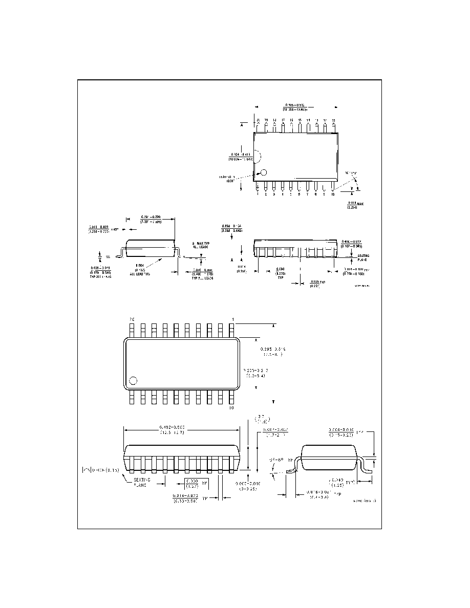
Physical Dimensions
inches (millimeters) unless otherwise noted
20-Lead Small Outline Integrated Circuit (SOIC), JEDEC MS-013, 0.300" Wide
Package Number M20B
20-Lead Small Outline Package (SOP), EIAJ TYPE II, 5.3mm Wide
Package Number M20D
www.fairchildsemi.com
8
MM
74
H
C
T3
73
· MM
74HCT374
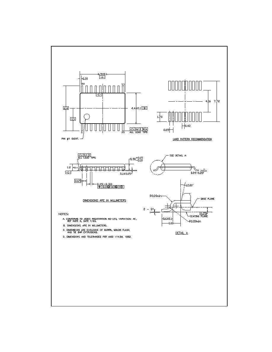
Physical Dimensions
inches (millimeters) unless otherwise noted (Continued)
20-Lead Thin Shrink Small Outline Package (TSSOP), JEDEC MO-153, 4.4mm Wide
Package Number MTC20
Fairchild does not assume any responsibility for use of any circuitry described, no circuit patent licenses are implied and Fairchild reserves the right at any time without notice to change said circuitry and specifications.
MM74HCT373
· MM74HCT374
3-ST
A
T
E Oct
a
l
D-T
ype L
a
tc
h
· 3-
ST
A
T
E
Octal
D-
T
ype
Fl
ip-
F
lop
LIFE SUPPORT POLICY
FAIRCHILD'S PRODUCTS ARE NOT AUTHORIZED FOR USE AS CRITICAL COMPONENTS IN LIFE SUPPORT
DEVICES OR SYSTEMS WITHOUT THE EXPRESS WRITTEN APPROVAL OF THE PRESIDENT OF FAIRCHILD
SEMICONDUCTOR CORPORATION. As used herein:
1. Life support devices or systems are devices or systems
which, (a) are intended for surgical implant into the
body, or (b) support or sustain life, and (c) whose failure
to perform when properly used in accordance with
instructions for use provided in the labeling, can be rea-
sonably expected to result in a significant injury to the
user.
2. A critical component in any component of a life support
device or system whose failure to perform can be rea-
sonably expected to cause the failure of the life support
device or system, or to affect its safety or effectiveness.
www.fairchildsemi.com
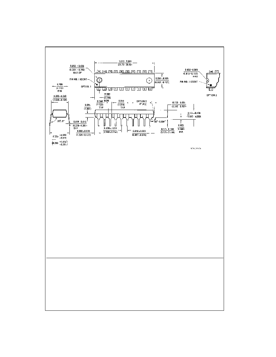
Physical Dimensions
inches (millimeters) unless otherwise noted (Continued)
20-Lead Plastic Dual-In-Line Package (PDIP), JEDEC MS-001, 0.300" Wide
Package Number N20A